ChipApex | Global Electronic Components Supplier

SEARCH
Search Product
Search Post
— IC芯片 | 连接器 | 传感器 | 被动器件 —
Search productSearch post
— IC芯片 | 连接器 | 传感器 | 被动器件 —
Consult the customer manager about the wholesale price.
consultation hotline:86-132-6715-2157
email:[email protected]
Contact the product manager for consultation. One-stop consultation is available.
Do you want a lower wholesale price? Please send us your inquiry and we will reply immediately.
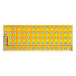
EPC2100 is listed in the FET, MOSFET Arrays range at ChipApex. The manufacturer field lists EPC. Its product description is MOSFET 2N-CH 30V 10A DIE. Review the specifications below when checking this part for your BOM.
The EPC2100 is an enhancement-mode GaN power transistor half-bridge die featuring a 30 V drain-to-source voltage rating. It integrates two N-channel eGaN FETs: Q1 with a maximum on-resistance of 8.2 mΩ and continuous current of 10 A, and Q2 with a maximum on-resistance of 2.1 mΩ and continuous current of 40 A. The device operates within a junction temperature range of -40°C to 150°C. Key electrical parameters include a gate threshold voltage of 2.5 V (max) and zero reverse recovery charge. The component is supplied in passivated die form with solder bumps for surface mount assembly.
Verify the specific lot date code and manufacturing year indicated by the laser markings on the die before integration. Confirm that the receiving facility has appropriate moisture sensitivity level handling procedures, as the device is classified as MSL 1. Ensure the solder paste composition matches the recommended SAC305 Type 4 specification for optimal bump attachment.
Select this component when designing compact half-bridge topologies requiring 30 V operation. Evaluate the thermal resistance values against your PCB copper pad area, as junction-to-ambient performance depends heavily on the mounting substrate. Consider the distinct current capabilities of Q1 and Q2 to optimize the duty cycle and load distribution within the circuit design.
This component belongs to the Efficient Power Conversion eGaN family of enhancement-mode transistors. It utilizes Gallium Nitride grown on silicon wafers processed with standard CMOS equipment. The technology leverages high electron mobility to achieve low on-state resistance compared to traditional silicon MOSFETs.
No official substitute part numbers are documented in the datasheet. Designers replacing silicon MOSFETs should utilize the EPC GaN Power Bench cross-reference tool to identify suitable alternatives based on specific operating conditions.
The datasheet specifies a maximum gate-to-source voltage of +6 V and a minimum of -4 V. Typical operation uses 5 V for the ON state.
The device is supplied in passivated die form with solder bumps, arranged in an 8 mm pitch, 12 mm wide tape on a 7-inch reel.
No, the lateral device structure does not contain a p-n body diode. It exhibits zero reverse recovery charge (QRR).
Explore related parts through FETs, MOSFETs, Transistors, Discrete Semiconductor Products, all product categories.
 EPC2100

The activity of extra discounts on wholesale prices is in full swing…
Please fill in your contact information and we will send you the latest wholesale price list.