ChipApex | Global Electronic Components Supplier

SEARCH
Search Product
Search Post
— IC芯片 | 连接器 | 传感器 | 被动器件 —
Search productSearch post
— IC芯片 | 连接器 | 传感器 | 被动器件 —
Consult the customer manager about the wholesale price.
consultation hotline:86-132-6715-2157
email:[email protected]
Contact the product manager for consultation. One-stop consultation is available.
Do you want a lower wholesale price? Please send us your inquiry and we will reply immediately.
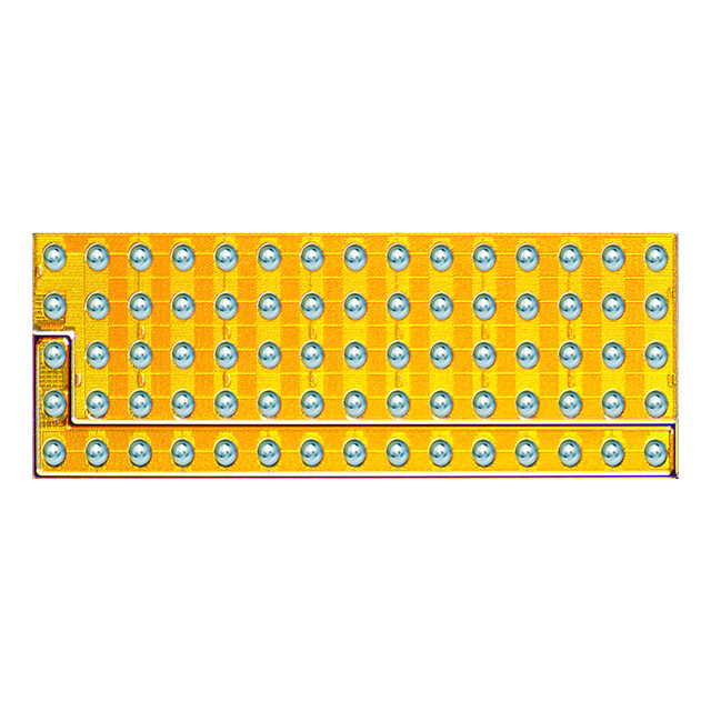
EPC2105 is listed in the FET, MOSFET Arrays range at ChipApex. The manufacturer field lists EPC. Its product description is MOSFET 2N-CH 80V 9.5A/38A DIE. Review the specifications below when checking this part for your BOM.
The EPC2105 is an enhancement-mode Gallium Nitride (GaN) power transistor configured as a half-bridge. It integrates two N-channel GaNFETs on a single die with dimensions of 6.05 x 2.3 mm. The high-side device (Q1) features a maximum drain-to-source voltage (VDS) of 80 V, a continuous drain current (ID) of 10 A at 25°C, and a typical on-resistance (RDS(on)) of 14.5 mΩ. The low-side device (Q2) supports a continuous ID of 40 A with a typical RDS(on) of 3.6 mΩ under the same conditions. Both devices operate within a junction temperature range of -40°C to 150°C.
Verify that the component is received in tape and reel format, as the EPC2105 is supplied exclusively in passivated die form with solder bumps. Confirm the presence of the orientation dot and check laser markings for lot date codes. Ensure handling procedures account for the bare die nature of the package to prevent damage during assembly.
Select this component when a compact half-bridge solution is required for high-frequency operation. Consider the distinct current ratings between Q1 and Q2; Q1 is suited for lower current paths while Q2 handles higher currents. Evaluate the thermal management requirements based on the specified junction-to-board and junction-to-case thermal resistances for the target application environment.
The EPC2105 belongs to the eGaN FET family manufactured by Efficient Power Conversion Corporation. It utilizes Gallium Nitride grown on silicon wafers processed with standard CMOS equipment. This technology leverages high electron mobility to achieve low on-resistance and fast switching speeds compared to traditional silicon MOSFETs.
No official substitute part numbers are listed in the datasheet. When evaluating alternatives, ensure the replacement matches the 80 V rating and provides comparable thermal characteristics. Verify that the new component supports surface mount assembly via solder bumps or compatible land patterns if direct footprint substitution is intended.
The datasheet specifies a gate-to-source voltage (VGS) of 5 V for measuring on-resistance and gate charge. The absolute maximum ratings allow for a positive VGS of 6 V and a negative VGS of -4 V.
The device is supplied only in passivated die form with solder bumps. It is packed in an 8 mm pitch, 12 mm wide tape on a 7-inch reel.
Yes, it features a majority carrier diode which results in zero reverse recovery charge (QRR).
Explore related parts through FETs, MOSFETs, Transistors, Discrete Semiconductor Products, all product categories.
 EPC2105

The activity of extra discounts on wholesale prices is in full swing…
Please fill in your contact information and we will send you the latest wholesale price list.