ChipApex | Global Electronic Components Supplier
SEARCH
Search Product
Search Post
— IC芯片 | 连接器 | 传感器 | 被动器件 —
Search productSearch post
— IC芯片 | 连接器 | 传感器 | 被动器件 —
Consult the customer manager about the wholesale price.
consultation hotline:86-132-6715-2157
email:[email protected]
Contact the product manager for consultation. One-stop consultation is available.
Do you want a lower wholesale price? Please send us your inquiry and we will reply immediately.
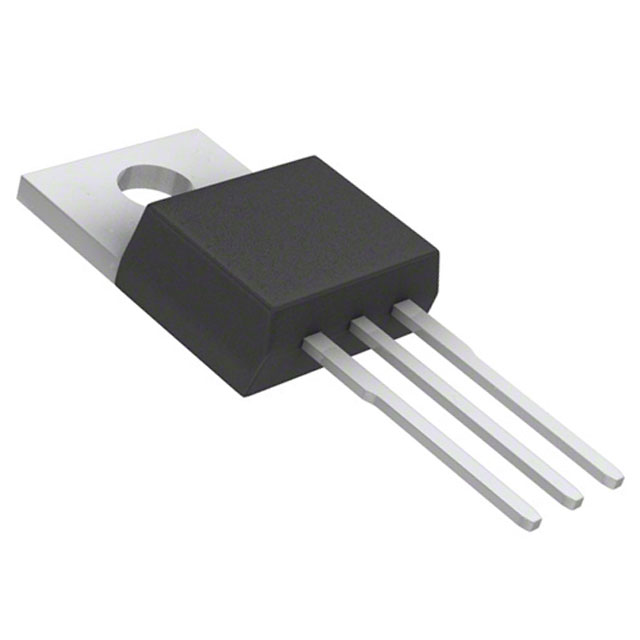
The FCP190N65S3 is a single N-channel power MOSFET from the onsemi SuperFET III series, utilizing charge balance technology for high-voltage superjunction performance. It features a 650V drain-source breakdown voltage and a maximum continuous drain current of 20A at case temperature of 25°C. The device offers a typical on-resistance of 190mΩ at VGS=10V and a gate charge of 34nC. Packaged in a TO-220-3 through-hole configuration, it supports a junction temperature range from -55°C to +150°C with a power dissipation rating of 36W.
Verify component authenticity through authorized distribution channels due to potential counterfeit risks. Confirm RoHS compliance status via official datasheets before integration. Ensure thermal management design accommodates the specified power dissipation limits within the operating temperature range. Validate package pinout compatibility with existing PCB footprints during the procurement phase.
Select this component for designs requiring high voltage isolation with efficient switching capabilities. The 190mΩ on-resistance balances conduction loss against gate drive requirements. Consider the TO-220-3 package for applications needing robust mechanical mounting and effective heat sinking. Evaluate system efficiency needs against the specific gate charge characteristics for optimal driver selection.
This part belongs to the SuperFET III family, representing an evolution in silicon superjunction MOSFET technology. The series integrates optimized cell structures to minimize both RDS(on) and Qg. This specific model targets medium-power conversion stages where reliability and thermal performance are critical constraints for long-term system operation.
The NTPF190N65S3HF is a documented alternative offering similar electrical specifications within the same manufacturer portfolio. Verify pinout compatibility and thermal resistance values when substituting to ensure circuit integrity without redesign.
 FCP190N65S3
The activity of extra discounts on wholesale prices is in full swing…
Please fill in your contact information and we will send you the latest wholesale price list.