 ChipApex | Global Electronic Components Supplier

SEARCH
Search Product
Search Post
— IC芯片 | 连接器 | 传感器 | 被动器件 —
Search productSearch post
— IC芯片 | 连接器 | 传感器 | 被动器件 —
Consult the customer manager about the wholesale price.
consultation hotline:86-132-6715-2157
email:[email protected]
Contact the product manager for consultation. One-stop consultation is available.
Do you want a lower wholesale price? Please send us your inquiry and we will reply immediately.
FDC6305N is listed in the FET, MOSFET Arrays range at ChipApex. The manufacturer field lists onsemi. Its product description is MOSFET 2N-CH 20V 2.7A SSOT6. Review the specifications below when checking this part for your BOM.
The FDC6305N is a dual N-channel enhancement mode MOSFET manufactured by onsemi. It is housed in an SSOT-6 surface-mount package designed for low-voltage applications. The device features a drain-source breakdown voltage (Vds) of 25 V and a continuous drain current (Id) of 1 A. The typical on-resistance (Rds(on)) is specified at 180 mΩ with a gate-source voltage of 4.5 V. The gate threshold voltage ranges from 0.4 V to 1.2 V, enabling compatibility with standard logic levels. Operating temperatures span from -55°C to +150°C, with a total power dissipation rating of 900 mW.
Verify the specific ordering suffix against the manufacturer's official datasheet to ensure correct packaging and tape-and-reel specifications. Confirm RoHS compliance status and environmental declarations directly from the product documentation before procurement. Cross-reference the component marking code with the official identification guide to prevent counterfeit substitution during acquisition.
Select this component when a dual N-channel topology is required within an SSOT-6 package. Ensure the application current remains below the 1 A continuous limit and that the operating voltage does not exceed 25 V. Verify that the thermal environment supports the 900 mW power dissipation rating without exceeding the maximum junction temperature limits defined in the electrical characteristics table.
This part belongs to the FDC series of dual MOSFETs from onsemi, which are engineered for portable electronics and battery-powered devices. The series emphasizes small outline packages to maximize board space efficiency while maintaining reliable switching performance for low-voltage DC-DC converters and load management tasks.
Consult the official cross-reference list for verified substitutes. Ensure any alternative maintains the SSOT-6 package, 25 V rating, and dual N-channel configuration. Verify pinout compatibility to avoid circuit redesign.
The absolute maximum gate-source voltage is ±8 V.
Yes, it features fast switching times with typical rise and fall times around 8.5 ns.
The typical total gate charge is approximately 2.3 nC.
Explore related parts through FETs, MOSFETs, Transistors, Discrete Semiconductor Products, all product categories.
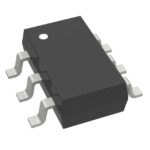 FDC6305N

The activity of extra discounts on wholesale prices is in full swing…
Please fill in your contact information and we will send you the latest wholesale price list.





