ChipApex | Global Electronic Components Supplier

SEARCH
Search Product
Search Post
— IC芯片 | 连接器 | 传感器 | 被动器件 —
Search productSearch post
— IC芯片 | 连接器 | 传感器 | 被动器件 —
Consult the customer manager about the wholesale price.
consultation hotline:86-132-6715-2157
email:[email protected]
Contact the product manager for consultation. One-stop consultation is available.
Do you want a lower wholesale price? Please send us your inquiry and we will reply immediately.
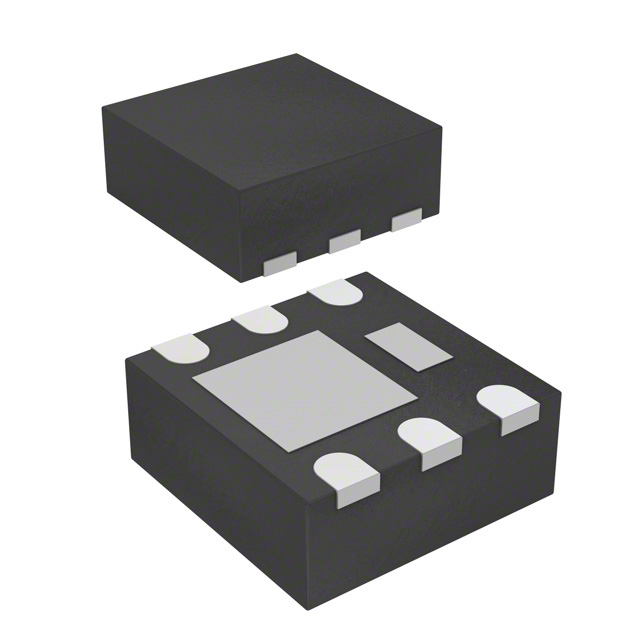
FDM2509NZ is listed in the FET, MOSFET Arrays range at ChipApex. The manufacturer field lists onsemi. Its product description is MOSFET 2N-CH 20V 8.7A MICRO 2X2. Review the specifications below when checking this part for your BOM.
The FDM2509NZ is a monolithic common drain dual N-Channel PowerTrench MOSFET designed for low-voltage applications. It features an optimized RDS(ON) at VGS = 2.5V and utilizes a MicroFET lead frame with all drains on one side. Key electrical parameters include a Drain-Source Voltage (VDSS) of 20V, a continuous Drain Current (ID) of 8.7A, and a maximum power dissipation of 2.2W. The device operates within a junction temperature range of -55°C to +150°C.
Verify the manufacturer origin as Fairchild Semiconductor, now part of onsemi, when sourcing this component. Confirm the specific revision level matches design requirements. Ensure the ordering suffix corresponds to the standard reel quantity of 3000 units. Check for RoHS compliance status if required by local regulations.
Select this component for circuits requiring a 20V rating and high current handling up to 8.7A. Consider the thermal resistance values based on the copper pad area used for mounting. Evaluate the gate threshold voltage variations across temperature ranges to ensure reliable switching at low gate voltages.
This device belongs to the PowerTrench family of MOSFETs, known for advanced process technology optimizing on-resistance. It is housed in a MicroFET 2x5 mm package, which provides a compact solution for space-constrained designs while maintaining efficient thermal performance through bottom drain contact.
Check for direct pin-compatible alternatives from the same manufacturer series. Verify that any substitute maintains the 20V VDSS rating and similar RDS(ON) characteristics at 2.5V and 4.5V gate drives. Ensure the replacement package dimensions match the existing footprint.
It serves only as protection against Electrostatic Discharge (ESD). It does not imply a gate overvoltage rating.
RθJA is the sum of junction-to-case and case-to-ambient resistance. The case thermal reference is defined as the solder mounting surface of the drain pins.
Typical turn-on delay is 11ns, rise time is 15ns, turn-off delay is 27ns, and fall time is 12ns under specified test conditions.
Explore related parts through FETs, MOSFETs, Transistors, Discrete Semiconductor Products, all product categories.
 FDM2509NZ

The activity of extra discounts on wholesale prices is in full swing…
Please fill in your contact information and we will send you the latest wholesale price list.