 ChipApex | Global Electronic Components Supplier

SEARCH
Search Product
Search Post
— IC芯片 | 连接器 | 传感器 | 被动器件 —
Search productSearch post
— IC芯片 | 连接器 | 传感器 | 被动器件 —
Consult the customer manager about the wholesale price.
consultation hotline:86-132-6715-2157
email:[email protected]
Contact the product manager for consultation. One-stop consultation is available.
Do you want a lower wholesale price? Please send us your inquiry and we will reply immediately.
FDS4501H is listed in the FET, MOSFET Arrays range at ChipApex. The manufacturer field lists onsemi. Its product description is MOSFET N/P-CH 30V/20V 9.3A 8SOIC. Review the specifications below when checking this part for your BOM.
The FDS4501H is a dual N-channel enhancement mode field effect transistor manufactured by onsemi. It features a maximum drain-source voltage of 30 V and a continuous drain current of 28 A at 25 °C. The device utilizes a DFN5x6 package with an exposed thermal pad for efficient heat dissipation. Key electrical characteristics include a maximum on-resistance of 7.5 mΩ at a gate-source voltage of 10 V and 9.5 mΩ at 5 V. The component supports a junction temperature range from -55 °C to +175 °C, making it suitable for high-power surface-mount applications requiring low conduction losses.
Verify the specific ordering suffix against the manufacturer's official datasheet to confirm pinout compatibility and thermal specifications. Ensure that the procurement channel provides traceable documentation confirming the component originates directly from onsemi or an authorized distribution network. Cross-reference the lot code with recent production change notices to validate material composition and manufacturing origin prior to integration into final assemblies.
Select this component when system requirements demand a dual N-channel topology within a constrained footprint. The 30 V rating and 28 A current capacity define the operational boundaries for load management. Evaluate the thermal resistance characteristics relative to the printed circuit board copper area to ensure junction temperatures remain within the specified maximum limits during continuous operation under full load conditions.
This part belongs to the FDS series of dual MOSFETs from onsemi, designed specifically for space-constrained power applications. The series integrates two matched transistors to simplify layout and reduce component count compared to discrete solutions. It serves as a standard solution for low-voltage, high-current switching tasks in consumer electronics and industrial equipment where efficiency and size are critical design parameters.
Direct replacements must match the 30 V / 28 A specification and DFN5x6 package dimensions. Verify that alternative dual N-channel devices offer comparable on-resistance values and thermal performance to maintain system efficiency and reliability without requiring redesign of the cooling infrastructure.
Explore related parts through FETs, MOSFETs, Transistors, Discrete Semiconductor Products, all product categories.
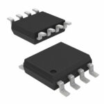 FDS4501H

The activity of extra discounts on wholesale prices is in full swing…
Please fill in your contact information and we will send you the latest wholesale price list.





