 ChipApex | Global Electronic Components Supplier

SEARCH
Search Product
Search Post
— IC芯片 | 连接器 | 传感器 | 被动器件 —
Search productSearch post
— IC芯片 | 连接器 | 传感器 | 被动器件 —
Consult the customer manager about the wholesale price.
consultation hotline:86-132-6715-2157
email:[email protected]
Contact the product manager for consultation. One-stop consultation is available.
Do you want a lower wholesale price? Please send us your inquiry and we will reply immediately.
FDW2507N is listed in the FET, MOSFET Arrays range at ChipApex. The manufacturer field lists onsemi. Its product description is MOSFET 2N-CH 20V 7.5A 8TSSOP. Review the specifications below when checking this part for your BOM.
The FDW2507N is a common drain N-Channel PowerTrench MOSFET designed for low-voltage applications. It features a TSSOP-8 package with isolated source and drain pins, optimizing thermal performance. The device supports a continuous drain current of 7.5 A at 25°C and withstands a drain-source voltage of 20 V. Key electrical parameters include an on-resistance of 19 mΩ at VGS = 4.5 V and 23 mΩ at VGS = 2.5 V. Gate threshold voltage ranges from 0.6 V to 1.5 V. Total gate charge is typically 20 nC at VGS = 4.5 V. Operating junction temperature spans -55°C to +150°C.
Verify the component origin carefully, as Fairchild Semiconductor was acquired by ON Semiconductor. Ensure the datasheet revision matches the specific manufacturing batch requirements. Confirm that the TSSOP-8 package marking corresponds to the '2507N' identifier. Check for authorized distributor status to avoid counterfeit parts, adhering to anti-counterfeiting policies regarding traceability and warranty coverage.
Select this component when a low-profile surface-mount solution is required for 20 V N-Channel switching. The specific optimization for 2.5 V gate drive makes it suitable for battery-powered systems where gate drive voltage may be limited. Verify that the 7.5 A continuous current rating and 1.6 W power dissipation capabilities align with the thermal design constraints of the target PCB layout.
This part belongs to the PowerTrench family of MOSFETs, originally developed by Fairchild Semiconductor before its acquisition by ON Semiconductor. The FDW2507N specifically utilizes a common drain configuration within a TSSOP-8 lead frame, distinguishing it from standard dual-channel or single-channel variants by providing dedicated thermal paths through isolated drain pins.
FDW2507NL
The maximum continuous drain current (ID) is 7.5 A at TA = 25°C.
The TSSOP-8 package has isolated source and drain pins. Thermal resistance (RθJA) is 77 °C/W on a 1in² pad of 2 oz copper and 114 °C/W on a minimum pad of 2 oz copper.
The gate threshold voltage (VGS(th)) ranges from a minimum of 0.6 V to a maximum of 1.5 V at ID = 250 µA.
Explore related parts through FETs, MOSFETs, Transistors, Discrete Semiconductor Products, all product categories.
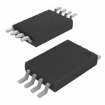 FDW2507N

The activity of extra discounts on wholesale prices is in full swing…
Please fill in your contact information and we will send you the latest wholesale price list.





