 ChipApex | Global Electronic Components Supplier

SEARCH
Search Product
Search Post
— IC芯片 | 连接器 | 传感器 | 被动器件 —
Search productSearch post
— IC芯片 | 连接器 | 传感器 | 被动器件 —
Consult the customer manager about the wholesale price.
consultation hotline:86-132-6715-2157
email:[email protected]
Contact the product manager for consultation. One-stop consultation is available.
Do you want a lower wholesale price? Please send us your inquiry and we will reply immediately.
FDW2601NZ is listed in the FET, MOSFET Arrays range at ChipApex. The manufacturer field lists onsemi. Its product description is MOSFET 2N-CH 30V 8.2A 8TSSOP. Review the specifications below when checking this part for your BOM.
The FDW2601NZ is a dual N-channel enhancement mode MOSFET manufactured using the PowerTrench process. It features a low-profile TSSOP-8 package with eight pins. The device supports a drain-source voltage of 30 V and a continuous drain current of 8.2 A at 25°C. The on-resistance is specified as 15 mΩ at VGS = 4.5 V and 20 mΩ at VGS = 2.5 V. Total gate charge is typically 20 nC at 4.5 V. The extended gate-source voltage range allows ±12 V operation. Thermal resistance junction-to-ambient is 77 °C/W on a minimum copper pad.
Verify component authenticity by checking the marking code '2601NZ' against the datasheet specifications. Confirm the package type is TSSOP-8 and the reel size is 13 inches with a tape width of 12 mm containing 2500 units per reel. Ensure the ordering suffix matches the required quantity and packaging format.
Select this component when designing portable electronics requiring dual N-channel switching with low on-resistance. The device is suitable for applications needing operation at VGS levels as low as 2.5 V. Consider the thermal resistance of 77 °C/W for heat dissipation requirements in steady-state conditions.
This part belongs to the PowerTrench series, utilizing advanced trench technology to minimize on-state resistance while maintaining low gate charge. Originally produced by Fairchild Semiconductor, it is designed for superior switching performance in portable electronic applications.
Consult official cross-reference lists or distributor databases for verified substitute part numbers from Fairchild or other manufacturers before implementation.
The absolute maximum gate-source voltage rating is ±12 V.
The on-resistance is 15 mΩ maximum at VGS = 4.5 V and 20 mΩ maximum at VGS = 2.5 V.
The device provides a typical Human Body Model (HBM) ESD protection level of 3.5 kV.
Explore related parts through FETs, MOSFETs, Transistors, Discrete Semiconductor Products, all product categories.
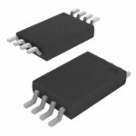 FDW2601NZ

The activity of extra discounts on wholesale prices is in full swing…
Please fill in your contact information and we will send you the latest wholesale price list.





