ChipApex | Global Electronic Components Supplier
SEARCH
Search Product
Search Post
— IC芯片 | 连接器 | 传感器 | 被动器件 —
Search productSearch post
— IC芯片 | 连接器 | 传感器 | 被动器件 —
Consult the customer manager about the wholesale price.
consultation hotline:86-132-6715-2157
email:[email protected]
Contact the product manager for consultation. One-stop consultation is available.
Do you want a lower wholesale price? Please send us your inquiry and we will reply immediately.
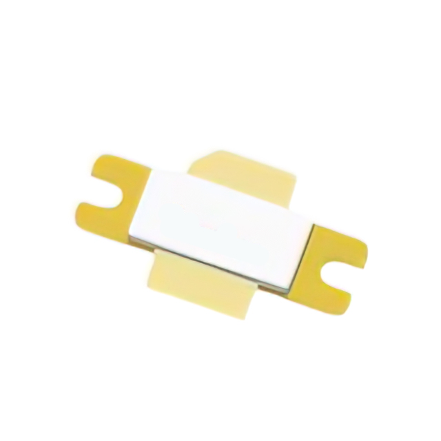
The GTVA107001EC-V1-R0 is a 700-watt GaN on SiC high electron mobility transistor (HEMT) designed for the DC to 1.4 GHz frequency band. It utilizes H-36248-2 bolt-down flange packaging and operates at a drain voltage of 50 V. The device delivers an output power of 890 W with a typical gain of 18 dB and a drain efficiency of 75% under pulsed CW conditions at 1030 MHz. Key electrical parameters include a drain-source breakdown voltage of 150 V, a gate threshold voltage of -3 V, and a maximum junction temperature of 225 °C.
Verify the specific ordering suffix against the manufacturer's official documentation to ensure correct package type and shipping quantity. Confirm that the required thermal interface materials and mounting hardware are compatible with the H-36248-2 flange dimensions. Ensure handling procedures strictly adhere to ESD sensitivity guidelines due to the device's classification as an electrostatic discharge sensitive component.
Select this component when designing amplifiers requiring high output power within the L-band spectrum. Evaluate thermal management requirements based on the specified junction-to-case thermal resistance values. Consider the input matching feature to reduce external component count. Verify that the operating duty cycle and pulse width align with the published performance characteristics to maintain reliability.
This part belongs to MACOM's GTVA series of high-power GaN HEMTs. It shares core technology with the GTVA107001FC variant, which utilizes an earless flange package. Both variants target similar military and communications applications but differ in mechanical mounting configurations. The EC designation specifically denotes the H-36248-2 package style.
GTVA107001FC-V1-R0
The recommended gate quiescent voltage is -3.2 V when the drain-source voltage is 50 V and the drain current is 0.10 A.
Yes, the datasheet provides typical performance data for both pulsed CW and continuous wave modes, including small signal gain and input return loss for CW operation.
The thermal resistance from junction to case is 0.21 °C/W at a case temperature of 85 °C with 334 W dissipation, or 0.25 °C/W at 85 °C with 254 W dissipation using Mode-S signal.
 GTVA107001EC-V1-R0
The activity of extra discounts on wholesale prices is in full swing…
Please fill in your contact information and we will send you the latest wholesale price list.