 ChipApex | Global Electronic Components Supplier

SEARCH
Search Product
Search Post
— IC芯片 | 连接器 | 传感器 | 被动器件 —
Search productSearch post
— IC芯片 | 连接器 | 传感器 | 被动器件 —
Consult the customer manager about the wholesale price.
consultation hotline:86-132-6715-2157
email:[email protected]
Contact the product manager for consultation. One-stop consultation is available.
Do you want a lower wholesale price? Please send us your inquiry and we will reply immediately.
IRF7309PBF is listed in the FET, MOSFET Arrays range at ChipApex. The manufacturer field lists Infineon Technologies. Its product description is MOSFET N/P-CH 30V 4A/3A 8SO. Review the specifications below when checking this part for your BOM.
The IRF7309PBF is a dual MOSFET from Infineon Technologies, integrating one N-channel and one P-channel enhancement-mode field-effect transistor within a single SOIC-8 surface-mount package. Designed for low-voltage applications, it features a drain-source breakdown voltage of 30 V. The device supports continuous drain currents of approximately 4 A for the N-channel and 3 A for the P-channel configurations. It exhibits a typical on-resistance of 50 mΩ at 10 V gate drive, enabling efficient power switching with minimal conduction losses in compact circuit designs.
Verify the specific suffix against the manufacturer's official documentation to confirm pinout compatibility and electrical tolerances. Ensure the selected variant matches the required package style and RoHS compliance status for your manufacturing process. Cross-reference the part number with current Infineon datasheets to validate availability and any recent design changes before finalizing procurement plans.
Select this component when a design requires both N-type and P-type switching capabilities within a constrained footprint. Evaluate the 30 V voltage rating against the system's maximum operating voltage to ensure adequate headroom. Consider the 50 mΩ on-resistance for thermal management calculations, as lower resistance reduces heat generation during continuous conduction periods in power-sensitive applications.
This component belongs to Infineon's portfolio of discrete power semiconductors designed for general-purpose switching. It utilizes silicon technology optimized for cost-effective mass production while maintaining high reliability standards. The dual configuration allows designers to implement bridge drivers or level shifters without sourcing separate components, streamlining the bill of materials for low-power electronic systems.
Consult official cross-reference lists for verified substitutes. Ensure any alternative maintains identical pin assignments and voltage ratings to prevent circuit damage during replacement.
The absolute maximum gate-source voltage rating is typically ±20 V. Exceeding this limit may damage the gate oxide layer.
Yes, both the N-channel and P-channel transistors contain intrinsic body diodes that conduct current when the device is reverse-biased.
The on-resistance decreases as the gate-source voltage increases. The specified value of 50 mΩ is measured at a gate drive of 10 V.
Explore related parts through FETs, MOSFETs, Transistors, Discrete Semiconductor Products, all product categories.
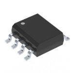 IRF7309PBF

The activity of extra discounts on wholesale prices is in full swing…
Please fill in your contact information and we will send you the latest wholesale price list.





