 ChipApex | Global Electronic Components Supplier

SEARCH
Search Product
Search Post
— IC芯片 | 连接器 | 传感器 | 被动器件 —
Search productSearch post
— IC芯片 | 连接器 | 传感器 | 被动器件 —
Consult the customer manager about the wholesale price.
consultation hotline:86-132-6715-2157
email:[email protected]
Contact the product manager for consultation. One-stop consultation is available.
Do you want a lower wholesale price? Please send us your inquiry and we will reply immediately.
IRF7342QTRPBF is listed in the FET, MOSFET Arrays range at ChipApex. The manufacturer field lists Infineon Technologies. Its product description is MOSFET 2P-CH 55V 3.4A 8SO. Review the specifications below when checking this part for your BOM.
The IRF7342QTRPBF is a dual P-channel HEXFET power MOSFET in an SO-8 surface-mount package. It features a -55V drain-source voltage and a maximum on-resistance of 0.105Ω at VGS=-10V. The device supports a continuous drain current of -3.4A at 25°C case temperature, with a pulsed current rating of -27A. It operates within a junction temperature range of -55°C to +150°C and includes an integral body diode.
Verify the specific ordering suffix 'QTR' corresponds to the Tape & Reel packaging format as documented in the official datasheet. Confirm that the component meets Industrial qualification standards per JEDEC guidelines. Ensure the selected variant aligns with the required lead-free specifications and moisture sensitivity level requirements for the intended manufacturing process.
Select this component when a compact dual P-channel solution is required for low-voltage power stages. Evaluate the thermal resistance and derating curves against the expected ambient conditions. Consider the gate charge and switching times for high-frequency applications. Verify that the -55V breakdown voltage provides adequate margin for the target circuit topology.
This part belongs to the Infineon HEXFET family, utilizing advanced processing techniques to achieve low on-resistance. The SO-8 package provides enhanced thermal performance compared to standard packages. The dual configuration allows for efficient implementation of half-bridge or synchronous rectifier topologies while minimizing printed circuit board footprint.
IRF7342PBF (Tube/Bulk packaging)
The device has a single-pulse avalanche energy rating of 114 mJ.
Yes, the MOSFET symbol indicates an integral reverse p-n junction diode between the source and drain.
The peak diode recovery dv/dt rating is specified as 5.0 V/ns.
Explore related parts through FETs, MOSFETs, Transistors, Discrete Semiconductor Products, all product categories.
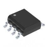 IRF7342QTRPBF

The activity of extra discounts on wholesale prices is in full swing…
Please fill in your contact information and we will send you the latest wholesale price list.





