 ChipApex | Global Electronic Components Supplier

SEARCH
Search Product
Search Post
— IC芯片 | 连接器 | 传感器 | 被动器件 —
Search productSearch post
— IC芯片 | 连接器 | 传感器 | 被动器件 —
Consult the customer manager about the wholesale price.
consultation hotline:86-132-6715-2157
email:[email protected]
Contact the product manager for consultation. One-stop consultation is available.
Do you want a lower wholesale price? Please send us your inquiry and we will reply immediately.
IRF7379TR is listed in the FET, MOSFET Arrays range at ChipApex. The manufacturer field lists Infineon Technologies. Its product description is MOSFET N/P-CH 30V 5.8A/4.3A 8SO. Review the specifications below when checking this part for your BOM.
The IRF7379TR is a dual N-channel and P-channel enhancement mode MOSFET from the HEXFET family, housed in an SO-8 surface-mount package. It features a drain-source voltage of 30V for both channels. The N-channel continuous drain current is 5.8A at 25°C, with a maximum on-resistance of 45mΩ at VGS=10V. The P-channel continuous drain current is 4.3A at 25°C, with a maximum on-resistance of 90mΩ at VGS=-10V. Power dissipation is rated at 2.5W, and the junction temperature range spans -55°C to +150°C.
Verify component authenticity through official manufacturer channels or authorized distributors. Confirm that the received part matches the specific IRF7379TR designation and packaging requirements. Review the datasheet for handling precautions and soldering guidelines to ensure proper integration into the target assembly process.
Select this component when a compact dual MOSFET solution is required for low-voltage switching applications. The SO-8 package offers a balance between thermal performance and board space savings compared to larger packages. Ensure the application current and voltage levels remain within the specified absolute maximum ratings for reliable operation.
This component belongs to the HEXFET power MOSFET series developed by International Rectifier, now part of Infineon Technologies. The series utilizes advanced processing techniques to deliver high-performance switching capabilities in a standardized surface-mount footprint suitable for consumer and industrial electronics.
IRF7379PbF
The maximum gate-to-source voltage is ±20V.
Yes, the SO-8 package is designed for vapor phase, infrared, or wave soldering techniques.
The typical total gate charge (Qg) for the N-channel is 25nC.
Explore related parts through FETs, MOSFETs, Transistors, Discrete Semiconductor Products, all product categories.
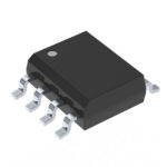 IRF7379TR

The activity of extra discounts on wholesale prices is in full swing…
Please fill in your contact information and we will send you the latest wholesale price list.





