 ChipApex | Global Electronic Components Supplier

SEARCH
Search Product
Search Post
— IC芯片 | 连接器 | 传感器 | 被动器件 —
Search productSearch post
— IC芯片 | 连接器 | 传感器 | 被动器件 —
Consult the customer manager about the wholesale price.
consultation hotline:86-132-6715-2157
email:[email protected]
Contact the product manager for consultation. One-stop consultation is available.
Do you want a lower wholesale price? Please send us your inquiry and we will reply immediately.
IRF7509TR is listed in the FET, MOSFET Arrays range at ChipApex. The manufacturer field lists Infineon Technologies. Its product description is MOSFET N/P-CH 30V 2.7A/2A MICRO8. Review the specifications below when checking this part for your BOM.
The IRF7509TR is a dual N-channel and P-channel enhancement mode MOSFET from the HEXFET series, utilizing Fifth Generation V technology. It features an ultra-low on-resistance of 135 mΩ for the N-channel and 200 mΩ for the P-channel at VGS = 10V. The device operates with a drain-source voltage of ±30 V and supports continuous drain currents of 2.7 A (N-channel) and -2.0 A (P-channel) at 25°C. Packaged in a compact Micro8 outline with a low profile under 1.1 mm, it offers fast switching capabilities and a maximum junction temperature rating of 150°C.
Verify that the ordering suffix matches the specific tape and reel configuration required for automated assembly processes. Confirm the component is lead-free and complies with relevant environmental directives before finalizing procurement orders. Ensure the supplier provides valid traceability documentation for the manufacturing batch.
Select this component when a dual N/P channel configuration is necessary within a restricted physical footprint. Evaluate the thermal resistance characteristics against the expected power dissipation requirements. Consider the gate charge specifications to ensure compatibility with the driving circuit's switching speed limitations.
This part belongs to the HEXFET Power MOSFET family, which employs advanced processing to deliver ruggedized device designs with fast switching speeds. The Micro8 package represents a significant reduction in size compared to standard SOIC outlines, offering the smallest footprint available in its class for surface mount applications.
Consult official cross-reference data for verified substitutes. Generic replacements may differ in pinout or electrical ratings.
The maximum operating junction temperature range extends up to +150°C.
Yes, the datasheet specifies peak diode recovery dv/dt ratings, indicating the presence of intrinsic body diodes for both channels.
The typical total gate charge is approximately 16 nC at a gate-to-source voltage of 10V.
Explore related parts through FETs, MOSFETs, Transistors, Discrete Semiconductor Products, all product categories.
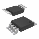 IRF7509TR

The activity of extra discounts on wholesale prices is in full swing…
Please fill in your contact information and we will send you the latest wholesale price list.





