 ChipApex | Global Electronic Components Supplier

SEARCH
Search Product
Search Post
— IC芯片 | 连接器 | 传感器 | 被动器件 —
Search productSearch post
— IC芯片 | 连接器 | 传感器 | 被动器件 —
Consult the customer manager about the wholesale price.
consultation hotline:86-132-6715-2157
email:[email protected]
Contact the product manager for consultation. One-stop consultation is available.
Do you want a lower wholesale price? Please send us your inquiry and we will reply immediately.
IRF8513TRPBF is listed in the FET, MOSFET Arrays range at ChipApex. The manufacturer field lists Infineon Technologies. Its product description is MOSFET 2N-CH 30V 8A/11A 8SO. Review the specifications below when checking this part for your BOM.
The IRF8513TRPBF is a dual N-channel HEXFET power MOSFET in an SO-8 package. It integrates two optimized transistors: Q1 (Control FET) with Rds(on) max of 15.5mΩ at Vgs=10V and Id=8.0A, and Q2 (Synchronous FET) with Rds(on) max of 12.7mΩ at Vgs=10V and Id=11A. Both channels feature a 30V drain-source breakdown voltage and a ±20V gate-source rating. The device supports continuous currents up to 8.0A (Q1) and 11A (Q2) at 25°C, with pulsed currents reaching 64A and 88A respectively. Total gate charge is typically 5.7nC for Q1 and 7.6nC for Q2.
Verify the component status as discontinued or obsolete through official manufacturer channels before finalizing design-in decisions. Confirm that the specific tape-and-reel packaging variant matches the required manufacturing automation standards. Ensure compliance with current environmental directives such as RoHS and halogen-free requirements by checking the latest datasheet revision. Validate thermal management capabilities against the junction-to-ambient resistance specifications provided in the official documentation.
Select this component for high-efficiency synchronous buck converters requiring compact dual-MOSFET integration. The distinct optimization of Q1 and Q2 allows tailored performance for control and synchronous roles. Evaluate thermal constraints carefully due to the SO-8 package limitations. Consider the low gate charge for driving efficiency in high-frequency operation. Ensure the 30V voltage rating provides sufficient headroom for the target application's input voltage range.
This part belongs to the HEXFET family utilizing advanced silicon technology. It represents a dual-transistor solution aimed at reducing board space compared to discrete implementations. The SO-8 package offers a balance between thermal dissipation and footprint size for consumer electronics. It is designed to replace separate N-channel MOSFETs in point-of-load architectures.
IRF8513PbF
Q1 is optimized as the Control FET with a maximum continuous drain current of 8.0A and Rds(on) of 15.5mΩ. Q2 is optimized as the Synchronous FET with a higher current rating of 11A and lower Rds(on) of 12.7mΩ.
Yes, the device is fully characterized for avalanche voltage and current, with guaranteed single-pulse avalanche energy ratings of 49mJ for Q1 and 70mJ for Q2.
The maximum gate-to-source voltage rating is ±20V for both channels.
Explore related parts through FETs, MOSFETs, Transistors, Discrete Semiconductor Products, all product categories.
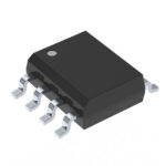 IRF8513TRPBF

The activity of extra discounts on wholesale prices is in full swing…
Please fill in your contact information and we will send you the latest wholesale price list.





