 ChipApex | Global Electronic Components Supplier

SEARCH
Search Product
Search Post
— IC芯片 | 连接器 | 传感器 | 被动器件 —
Search productSearch post
— IC芯片 | 连接器 | 传感器 | 被动器件 —
Consult the customer manager about the wholesale price.
consultation hotline:86-132-6715-2157
email:[email protected]
Contact the product manager for consultation. One-stop consultation is available.
Do you want a lower wholesale price? Please send us your inquiry and we will reply immediately.
IRF8915 is listed in the FET, MOSFET Arrays range at ChipApex. The manufacturer field lists Infineon Technologies. Its product description is MOSFET 2N-CH 20V 8.9A 8SO. Review the specifications below when checking this part for your BOM.
The IRF8915 is a dual N-channel HEXFET power MOSFET in an SO-8 package. It features a maximum drain-to-source voltage of 20 V and a continuous drain current of 8.9 A at 25°C. The device has a maximum on-resistance of 18.3 mΩ at VGS = 10V and 27 mΩ at VGS = 4.5V. Total gate charge is typically 4.9 nC at VGS = 4.5V, with a gate-drain charge of 1.7 nC. Maximum power dissipation is 2 W at 25°C, and the junction temperature range extends up to 150°C.
Verify the specific ordering suffix against official Infineon documentation to confirm package type and tape-and-reel specifications. Ensure the component meets RoHS compliance requirements if mandated by your design standards. Cross-reference the manufacturer part number with authorized distributors to validate authenticity and traceability before finalizing procurement.
Select this component for applications requiring a dual N-channel MOSFET solution in a space-constrained SO-8 footprint. The low gate charge supports high-frequency switching operations typical in POL converters. Evaluate thermal performance based on the specified junction-to-ambient resistance and ensure the operating environment stays within the -55°C to +150°C range.
This component belongs to the HEXFET family of power MOSFETs from Infineon Technologies. It utilizes Trench technology to achieve low on-resistance and fast switching speeds. The dual configuration allows for synchronous rectification or half-bridge topologies within a single package, optimizing board space and reducing interconnect parasitics in power conversion circuits.
Consult official cross-reference tools for verified substitutes. Ensure any replacement maintains the 20 V rating, SO-8 package dimensions, and dual N-channel configuration. Verify that thermal characteristics and gate charge parameters are compatible with the existing driver circuitry.
The maximum continuous drain current is 8.9 A at an ambient temperature of 25°C.
Yes, the device is fully characterized for avalanche voltage and current, allowing it to handle unclamped inductive switching events within specified limits.
The typical total gate charge (Qg) is 4.9 nC when measured at a gate-to-source voltage of 4.5V.
Explore related parts through FETs, MOSFETs, Transistors, Discrete Semiconductor Products, all product categories.
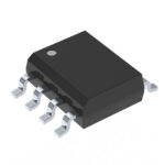 IRF8915

The activity of extra discounts on wholesale prices is in full swing…
Please fill in your contact information and we will send you the latest wholesale price list.





