ChipApex | Global Electronic Components Supplier

SEARCH
Search Product
Search Post
— IC芯片 | 连接器 | 传感器 | 被动器件 —
Search productSearch post
— IC芯片 | 连接器 | 传感器 | 被动器件 —
Consult the customer manager about the wholesale price.
consultation hotline:86-132-6715-2157
email:[email protected]
Contact the product manager for consultation. One-stop consultation is available.
Do you want a lower wholesale price? Please send us your inquiry and we will reply immediately.
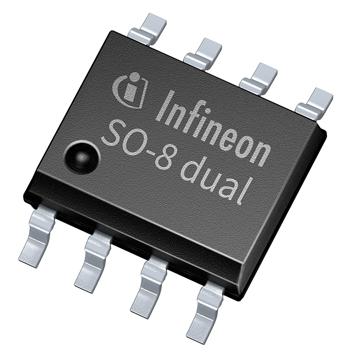
ISA250300C04LMDSXTMA1 is listed in the FET, MOSFET Arrays range at ChipApex. The manufacturer field lists Infineon Technologies. Its product description is ISA250300C04LMDSXTMA1. Review the specifications below when checking this part for your BOM.
The ISA250300C04LMDSXTMA1 is an OptiMOS™ 3 complementary dual power MOSFET in a PG-DSO-8 package. It integrates N-channel and P-channel transistors with V_DS ratings of 40 V and -40 V respectively. The N-channel offers R_DS(on) max of 25 mΩ at V_GS=10V and I_D max of 7.9 A. The P-channel provides R_DS(on) max of 30 mΩ at V_GS=-10V and I_D max of -7.8 A. Operating temperature range is -55 °C to 150 °C.
Verify the specific ordering suffix XTMA1 against official Infineon documentation to confirm tape-and-reel packaging specifications. Ensure the component meets RoHS compliance and halogen-free requirements as stated in the datasheet. Cross-reference the final datasheet revision 2.0 for accurate electrical parameters before procurement.
Select this component for designs requiring both N-type and P-type switching capabilities in a minimal space. The logic-level gate threshold voltage allows direct interfacing with standard logic outputs. Evaluate thermal dissipation requirements based on the specified junction-to-ambient thermal resistance values under your specific PCB layout conditions.
This part belongs to the OptiMOS™ 3 family of power transistors, designed for general-purpose switching applications. It utilizes advanced trench technology to achieve low on-resistance and fast switching speeds. The PG-DSO-8 package provides a robust solution for surface-mount assembly while maintaining high current handling capabilities.
Consult official cross-reference lists for verified substitutes. Ensure any replacement maintains identical pinout configuration, voltage ratings, and thermal performance characteristics to guarantee circuit compatibility without redesign.
The maximum continuous drain current (I_D) for the N-channel is 7.9 A at T_C = 25°C.
Yes, the product validation section confirms it is qualified according to JEDEC Standard.
The gate threshold voltage (V_GS(th)) ranges from 1.1 V to 2.7 V at I_D = 1000 μA.
Explore related parts through FETs, MOSFETs, Transistors, Discrete Semiconductor Products, all product categories.
 ISA250300C04LMDSXTMA1

The activity of extra discounts on wholesale prices is in full swing…
Please fill in your contact information and we will send you the latest wholesale price list.