ChipApex | Global Electronic Components Supplier
SEARCH
Search Product
Search Post
— IC芯片 | 连接器 | 传感器 | 被动器件 —
Search productSearch post
— IC芯片 | 连接器 | 传感器 | 被动器件 —
Consult the customer manager about the wholesale price.
consultation hotline:86-132-6715-2157
email:[email protected]
Contact the product manager for consultation. One-stop consultation is available.
Do you want a lower wholesale price? Please send us your inquiry and we will reply immediately.
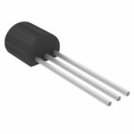
The J107 is an N-Channel Junction Field-Effect Transistor (JFET) switch manufactured by onsemi. It is housed in a TO-92 three-lead through-hole package and utilizes silicon technology. The device features a gate-source breakdown voltage of -25 V and a drain-source on resistance of 8 Ohms at zero gate voltage. Maximum power dissipation is rated at 625 mW, with a junction-to-ambient thermal resistance of 357 °C/W. The component operates within a temperature range of -55°C to +150°C.
Verify the current production status before procurement as this component may be discontinued. Confirm that the TO-92 package dimensions match your PCB footprint requirements. Ensure that the 8 Ohm on-resistance meets the specific voltage drop constraints of your application design. Check for updated ordering suffixes due to manufacturer integration changes.
Select the J107 when a low-cost, single-channel N-Channel JFET switch is required for moderate current applications. Compare its 8 Ohm on-resistance against other variants like the J105 or J106 if lower resistance is needed. Ensure the circuit design accommodates the -4.5 V maximum gate-source cut-off voltage to guarantee proper turn-off characteristics.
The J107 belongs to a family of N-Channel JFET switches that includes the J105 and J106 models. These components share similar packaging and basic electrical structures but differ in their specific on-resistance and cut-off voltage specifications. This series is designed for cost-effective switching solutions in consumer and industrial electronics.
The J105 and J106 are direct functional siblings within the same datasheet. The J105 offers lower on-resistance (3 Ohms), while the J106 provides intermediate characteristics (6 Ohms). Verify pinout compatibility and thermal derating requirements when substituting between these variants.

The activity of extra discounts on wholesale prices is in full swing…
Please fill in your contact information and we will send you the latest wholesale price list.