 ChipApex | Global Electronic Components Supplier
SEARCH
Search Product
Search Post
— IC芯片 | 连接器 | 传感器 | 被动器件 —
Search productSearch post
— IC芯片 | 连接器 | 传感器 | 被动器件 —
Consult the customer manager about the wholesale price.
consultation hotline:86-132-6715-2157
email:[email protected]
Contact the product manager for consultation. One-stop consultation is available.
Do you want a lower wholesale price? Please send us your inquiry and we will reply immediately.
The J309G is an N-channel depletion-mode Junction Field-Effect Transistor (JFET) designed for VHF and UHF amplifier applications. It features a TO-92 (CASE 29-11) package with Style 5 pin configuration: Pin 1 Drain, Pin 2 Source, Pin 3 Gate. Key electrical parameters include a Drain-Source Voltage (VDS) of 25 Vdc and a Gate-Source Voltage (VGS) of 25 Vdc. The Zero-Gate-Voltage Drain Current (IDSS) ranges from 12 mA to 30 mA at VDS = 10 Vdc. At 100 MHz, the Common-Gate Power Gain (Gpg) is typically 16 dB, and the Forward Transconductance (Re(yfs)) is typically 12 mmhos.
Verify the ordering suffix 'G' indicates a Pb-Free package as per onsemi documentation. Confirm the specific pin style (Style 5) matches the target circuit design. Ensure compliance with RoHS directives if required by the end application. Check for any specific handling precautions related to the TO-92 lead frame construction during assembly.
Select this component when a low-noise N-channel JFET is required for frequencies up to the UHF band. Compare IDSS ranges against circuit biasing requirements. Evaluate the typical 16 dB power gain at 100 MHz against system link budget needs. Consider the TO-92 package constraints for thermal dissipation in enclosed environments.
The J309G belongs to the J309/J310 family of N-channel depletion JFETs manufactured by onsemi. It serves as a preferred device choice for RF signal processing stages. The 'G' suffix denotes environmental compliance, specifically Pb-Free packaging, distinguishing it from older non-compliant variants while maintaining identical electrical specifications.
Public datasheets list the J309 as a direct replacement for discontinued Siliconix J309 units. Verify pinout compatibility (Drain-Source-Gate) when substituting. No other specific cross-reference part numbers are confirmed in the provided source material.
The J309G uses TO-92 Style 5 pinout: Pin 1 is Drain, Pin 2 is Source, and Pin 3 is Gate.
The typical Common-Source Forward Transconductance Re(yfs) is 12 mmhos at VDS = 10 Vdc, ID = 10 mAdc, and f = 100 MHz.
Yes, the 'G' suffix indicates that the device is available in Pb-Free packages compliant with onsemi's environmental strategy.
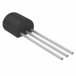 J309G
J309G
The activity of extra discounts on wholesale prices is in full swing…
Please fill in your contact information and we will send you the latest wholesale price list.





