ChipApex | Global Electronic Components Supplier
SEARCH
Search Product
Search Post
— IC芯片 | 连接器 | 传感器 | 被动器件 —
Search productSearch post
— IC芯片 | 连接器 | 传感器 | 被动器件 —
Consult the customer manager about the wholesale price.
consultation hotline:86-132-6715-2157
email:[email protected]
Contact the product manager for consultation. One-stop consultation is available.
Do you want a lower wholesale price? Please send us your inquiry and we will reply immediately.
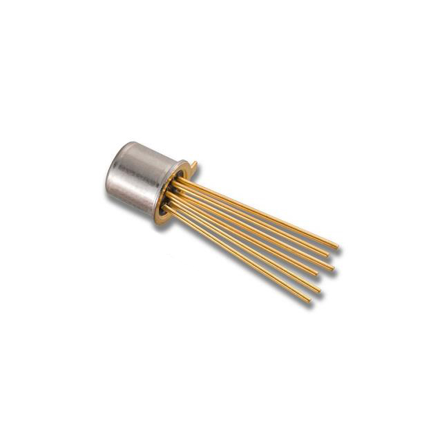
The LSK489 is a monolithic dual N-channel JFET amplifier featuring industry-low input capacitance and low noise. It offers an input voltage noise of 1.8 nV/√Hz at 1 kHz and a common source input capacitance of 4 pF. The device provides high CMRR (102 dB typical) and tight differential voltage matching. Available in TO-71 6L, SOIC 8L, and SOT-23 6L packages, it supports continuous power dissipation of 300 mW per side with a maximum gate-to-source voltage of 60 V.
Verify the specific grade (A or B) required for your design, as IDSS ranges differ between grades. Confirm package availability matches your PCB layout needs, as the TO-71 6L is pin-compatible with the LSK389. Check datasheet limits for custom selection codes if tighter electrical parameters are necessary for your application.
Select the LSK489 when low input capacitance is critical to minimize intermodulation distortion, rather than absolute lowest noise. Choose Grade A for tighter IDSS matching (ΔIDSS = 6mA) or Grade B for higher current ranges (ΔIDSS = 7mA). Ensure the operating temperature stays within -55°C to +150°C for reliable performance.
The LSK489 serves as a low-capacitance alternative to the LSK389 within Linear Integrated Systems' portfolio. While the LSK389 offers lower noise, the LSK489 provides significantly lower gate-to-drain capacitance (4pF vs 25pF). Both devices share identical pinouts and package options, allowing for interchangeable use in designs prioritizing speed and low distortion over minimal noise floor.
The LSK389 is a direct fit, form, and pin-compatible replacement. For single-channel requirements, consider the LSK189.
 LSK489 TO-71 6L ROHS
The activity of extra discounts on wholesale prices is in full swing…
Please fill in your contact information and we will send you the latest wholesale price list.