ChipApex | Global Electronic Components Supplier
SEARCH
Search Product
Search Post
— IC芯片 | 连接器 | 传感器 | 被动器件 —
Search productSearch post
— IC芯片 | 连接器 | 传感器 | 被动器件 —
Consult the customer manager about the wholesale price.
consultation hotline:86-132-6715-2157
email:[email protected]
Contact the product manager for consultation. One-stop consultation is available.
Do you want a lower wholesale price? Please send us your inquiry and we will reply immediately.
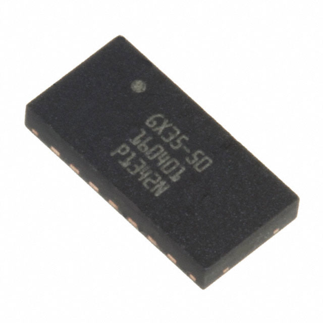
The MAGX-000035-05000P is a GaN on SiC depletion-mode (D-Mode) transistor designed for pulsed RF applications across the DC to 3.5 GHz frequency range. It features a thermally enhanced 3 x 6 mm 14-lead DFN plastic package and operates with a typical Class AB bias of 50 V. The device delivers a typical pulsed output power of 50 W at 1 ms pulse width and 10% duty cycle, achieving up to 66% drain efficiency. It supports high load mismatch tolerance, withstanding VSWR up to 10:1, and maintains reliability at junction temperatures up to 200°C.
Verify the specific ordering suffix to confirm packaging type; the 'P' suffix indicates bulk packaging, while other suffixes may denote reel or sample board configurations. Ensure compatibility with RoHS directives and moisture sensitivity level 1 requirements during storage and handling. Confirm that the design accommodates the required thermal management for the specified duty cycles and junction temperatures.
Select this component when high peak power in a small form factor is required for pulsed signals rather than continuous wave operation. Consider the 50 V typical bias requirement and the need for appropriate gate drive sequencing to prevent latch-up. Evaluate thermal resistance characteristics against the expected duty cycle and ambient temperature conditions to ensure junction temperature limits are not exceeded.
This part belongs to MACOM's MAGX series of wideband GaN transistors, which are engineered for high voltage and high power density. The series utilizes silicon carbide substrates to support superior thermal conductivity and breakdown voltage capabilities compared to standard silicon technologies.
MAGX-000035-05000TP
Set the gate voltage (VG) to pinch-off (typically -5 V), turn on the drain supply (VD) to nominal voltage (50 V), increase VG until the desired IDS current is reached, and then apply RF power.
The transistor demonstrates strong load mismatch stability and tolerance, capable of withstanding a VSWR of up to 5:1 for stability and up to 10:1 for tolerance under pulsed operating conditions.
The absolute maximum junction temperature is rated at 200°C, supported by internal stress buffer technology that ensures reliable operation at these elevated temperatures.
 MAGX-000035-05000P
The activity of extra discounts on wholesale prices is in full swing…
Please fill in your contact information and we will send you the latest wholesale price list.