ChipApex | Global Electronic Components Supplier
SEARCH
Search Product
Search Post
— IC芯片 | 连接器 | 传感器 | 被动器件 —
Search productSearch post
— IC芯片 | 连接器 | 传感器 | 被动器件 —
Consult the customer manager about the wholesale price.
consultation hotline:86-132-6715-2157
email:[email protected]
Contact the product manager for consultation. One-stop consultation is available.
Do you want a lower wholesale price? Please send us your inquiry and we will reply immediately.
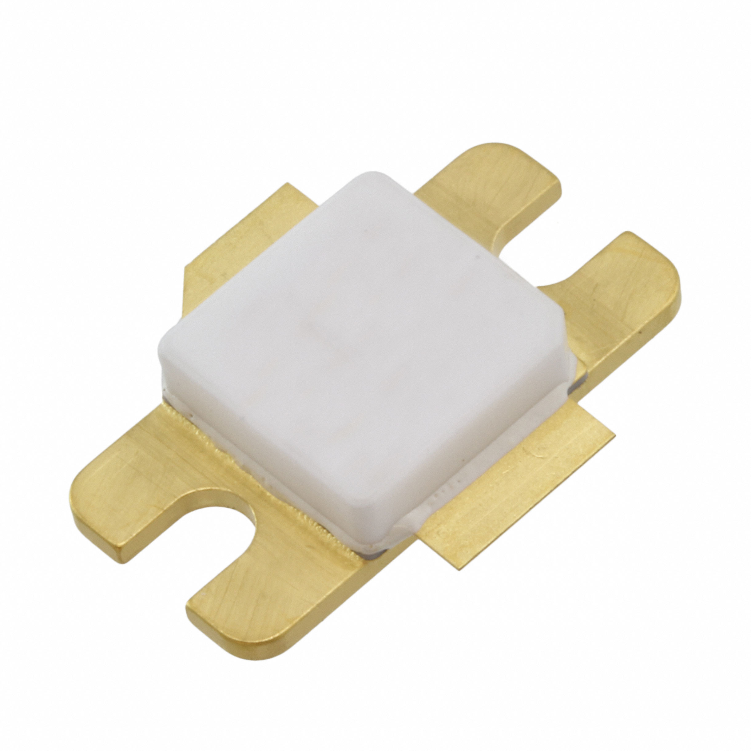
The MAGX-000912-250L00 is a GaN on SiC depletion-mode HEMT pulsed power transistor designed for the 960 MHz to 1215 MHz frequency range. It delivers a peak output power of 250 W with a 128 µs pulse width and 10% duty cycle. The device operates at a typical drain voltage of +50 V, providing a gain of approximately 18.7 dB and a drain efficiency up to 61.1%. It features an internally matched common-source configuration and robust load mismatch tolerance.
Verify the specific part number suffix against official MACOM documentation to confirm exact manufacturing revisions and testing conditions. Ensure that procurement channels provide original manufacturer traceability. Confirm compliance with RoHS directives and verify that the component meets the required moisture sensitivity level standards before integration into production assemblies.
Select this component for high-power pulsed RF applications requiring wide bandwidth in the L-band spectrum. The internal matching network simplifies circuit design by eliminating external impedance matching components. Evaluate thermal management requirements carefully, as junction temperature directly impacts long-term reliability and mean time to failure metrics under continuous pulsed operation.
This device belongs to the MAGX series of Gallium Nitride on Silicon Carbide power transistors from M/A-COM Technology Solutions. The series utilizes advanced wafer fabrication processes to achieve high gain, efficiency, and bandwidth. These transistors are specifically engineered to handle demanding avionics environments where traditional semiconductor technologies may lack sufficient breakdown voltage or operational stability.
Consult official MACOM documentation for verified substitute part numbers. Do not assume functional equivalence with other L-band transistors without verifying pinout compatibility, electrical specifications, and thermal characteristics against the original datasheet.
Set the gate voltage (VGS) to pinch-off, typically -5 V. Turn on the drain voltage (VDS) to the nominal 50 V. Increase VGS until the desired drain current is reached, then apply the RF power.
The transistor exhibits high ruggedness, maintaining stable operation with a source mismatch tolerance of 5:1 VSWR and a load mismatch tolerance of 10:1 VSWR.
The absolute maximum operating junction temperature is 250 °C. However, keeping the junction temperature below 200 °C significantly extends the Mean Time To Failure (MTTF).
 MAGX-000912-250L00
The activity of extra discounts on wholesale prices is in full swing…
Please fill in your contact information and we will send you the latest wholesale price list.