ChipApex | Global Electronic Components Supplier
SEARCH
Search Product
Search Post
— IC芯片 | 连接器 | 传感器 | 被动器件 —
Search productSearch post
— IC芯片 | 连接器 | 传感器 | 被动器件 —
Consult the customer manager about the wholesale price.
consultation hotline:86-132-6715-2157
email:[email protected]
Contact the product manager for consultation. One-stop consultation is available.
Do you want a lower wholesale price? Please send us your inquiry and we will reply immediately.
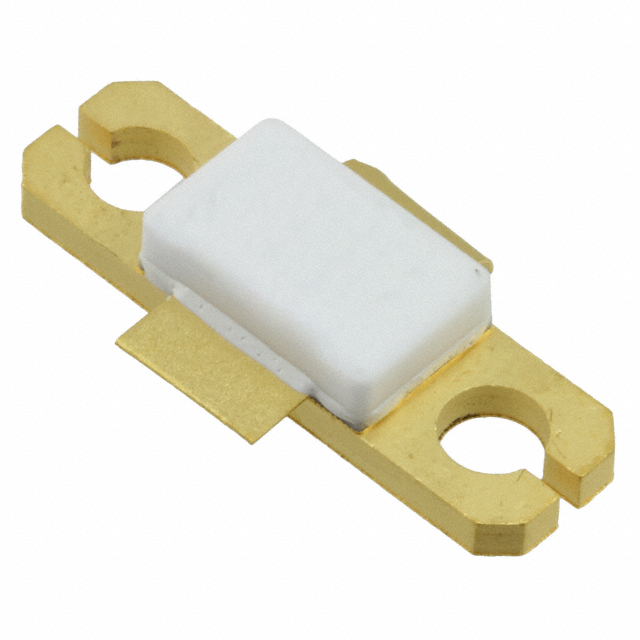
The MAGX-001220-100L00 is a Gallium Nitride on Silicon Carbide (GaN on SiC) depletion-mode HEMT transistor designed for high-power RF applications. It delivers a peak output power of 100 W with a typical value of 110 W across the 1.2 to 2.0 GHz frequency range. The device operates at a typical drain voltage of +50 V and achieves a drain efficiency of up to 55% under pulsed conditions (300 µs pulse width, 10% duty cycle). Key electrical parameters include a forward transconductance of 2.5 S, an output capacitance of 30.3 pF, and a gate threshold voltage ranging from -5 V to -2 V.
Verify component authenticity through authorized MACOM distributors or direct channels. Confirm RoHS compliance status and check for specific export classification requirements, as the device is classified as EAR99. Ensure handling procedures strictly follow electrostatic discharge (ESD) precautions due to the sensitivity of GaN devices. Review the latest datasheet revision for any updates to absolute maximum ratings or thermal resistance values before finalizing procurement specifications.
Select this component for designs requiring high peak power density within the 1.2 to 2.0 GHz band. The device is optimized for pulsed operations with a 300 µs pulse width and 10% duty cycle, though it supports general purpose CW use. Consider the thermal management capabilities of the Cu/Mo/Cu package when designing heat sinks. Ensure bias sequencing protocols are implemented to protect the gate-source junction during power-up and power-down cycles.
This part belongs to the MAGX series of GaN on SiC HEMT transistors from MACOM Technology Solutions. These components are engineered for next-generation RF power amplifiers, leveraging advanced wafer fabrication processes to deliver superior gain, efficiency, and bandwidth compared to older semiconductor technologies. The series targets demanding applications requiring reliability and high power output in compact form factors.
No public confirmed substitute part numbers are available in the provided documentation.
First set VGS to the pinch-off voltage (typically -5 V), then turn on VDS to the nominal voltage (+50 V). Next, increase VGS until the desired IDS current is reached, and finally apply the RF power.
The MTTF is specified as 600 years, provided the junction temperature remains below 200°C.
The transistor exhibits high ruggedness, maintaining stability with a VSWR-S of 5:1 and tolerating a VSWR-T of 10:1.
 MAGX-001220-100L00
The activity of extra discounts on wholesale prices is in full swing…
Please fill in your contact information and we will send you the latest wholesale price list.