 ChipApex | Global Electronic Components Supplier
SEARCH
Search Product
Search Post
— IC芯片 | 连接器 | 传感器 | 被动器件 —
Search productSearch post
— IC芯片 | 连接器 | 传感器 | 被动器件 —
Consult the customer manager about the wholesale price.
consultation hotline:86-132-6715-2157
email:[email protected]
Contact the product manager for consultation. One-stop consultation is available.
Do you want a lower wholesale price? Please send us your inquiry and we will reply immediately.
The MMBF4391LT1 is an N-channel JFET switching transistor manufactured by onsemi. It operates with a Drain-Source Voltage (VDS) of 30 Vdc and a Gate-Source Breakdown Voltage (V(BR)GSS) of 30 Vdc. The Zero-Gate-Voltage Drain Current (IDSS) ranges from 50 mA to 150 mA at VDS = 15 Vdc. The device features a maximum total device dissipation of 225 mW on an FR-5 board at 25°C ambient temperature, with a junction-to-ambient thermal resistance of 556 °C/W. It supports a junction and storage temperature range from -55°C to +150°C.
Verify the exact ordering suffix when purchasing. The 'G' suffix indicates a Pb-Free package. Confirm if the 'S' prefix is required for automotive qualification or specific manufacturing site controls. Ensure the requested part number matches the specific electrical characteristics defined in the datasheet, as variations exist within the MMBF4391L family.
Select this component based on the required IDSS range of 50 mA to 150 mA. Consider the 30 Vdc voltage ratings for drain-source and gate-source limits. Evaluate the thermal constraints, specifically the 225 mW dissipation limit, against the expected operating conditions. Verify packaging preferences between tape & reel and cut tape options.
This device belongs to the MMBF4391L, MMBF4392L, and MMBF4393L series of N-channel JFET switching transistors. These components are housed in SOT-23 packages (CASE 318). The series offers different IDSS ranges to accommodate various switching impedance requirements while maintaining consistent voltage ratings and package dimensions.
MMBF4391LT1G
Pin 1 is the Drain, Pin 2 is the Source, and Pin 3 is the Gate.
Yes, devices with the 'S' prefix are AEC-Q101 qualified and PPAP capable for automotive and other applications requiring unique site and control change requirements.
The maximum forward gate current (IG(f)) is rated at 50 mAdc.
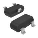 MMBF4391LT1
The activity of extra discounts on wholesale prices is in full swing…
Please fill in your contact information and we will send you the latest wholesale price list.





