ChipApex | Global Electronic Components Supplier

SEARCH
Search Product
Search Post
— IC芯片 | 连接器 | 传感器 | 被动器件 —
Search productSearch post
— IC芯片 | 连接器 | 传感器 | 被动器件 —
Consult the customer manager about the wholesale price.
consultation hotline:86-132-6715-2157
email:[email protected]
Contact the product manager for consultation. One-stop consultation is available.
Do you want a lower wholesale price? Please send us your inquiry and we will reply immediately.
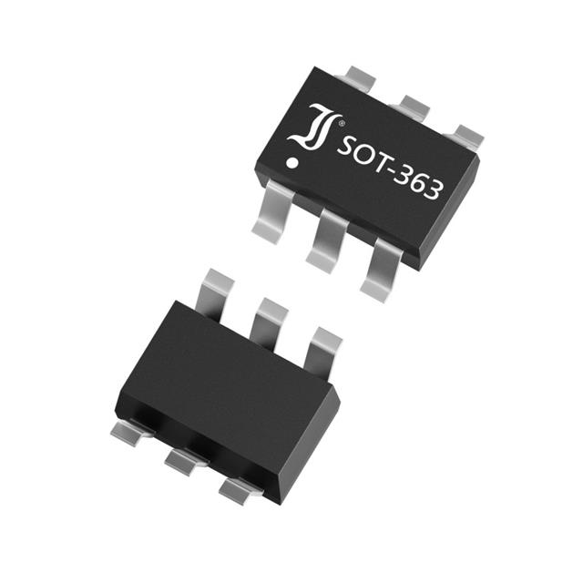
MMBT7002KDW is listed in the FET, MOSFET Arrays range at ChipApex. The manufacturer field lists Diotec Semiconductor. Its product description is MOSFET 2N-CH 60V 0.3A SOT363. Review the specifications below when checking this part for your BOM.
The Diotec Semiconductor MMBT7002KDW is a dual N-channel enhancement mode MOSFET housed in an SOT-363 surface-mount package. It features two independent FETs within a single compact footprint, designed for signal processing and logic level conversion. The device supports a drain-source voltage of 60 V and a continuous drain current of 300 mA per channel. Key electrical parameters include a maximum on-state resistance of 4 Ω at VGS = 5 V and 3 Ω at VGS = 10 V. Total power dissipation reaches 350 mW under standard mounting conditions, with a junction temperature range spanning from -55°C to +150°C.
Verify the specific ordering suffix when sourcing this component. The base model represents commercial grade performance. Suffixes such as -Q indicate AEC-Q101 compliance, while -AQ denotes AEC-Q101 qualification. Confirm that the delivered part matches the required automotive or commercial specification before integration into the design.
Select this component for designs requiring dual switching functions within a minimal board area. Ensure the driving circuit can supply sufficient gate voltage to achieve the specified low on-state resistance values. Consider the thermal resistance characteristics when determining heat dissipation requirements for high-frequency switching applications.
This component belongs to the broader 2N700X family of general-purpose N-channel MOSFETs. While sharing similar functional roles with single-channel variants like the 2N7002, the MMBT7002KDW distinguishes itself by offering dual isolation within a single surface-mount package. This makes it suitable for applications where space constraints necessitate multiple switching elements.
Direct replacements must match the SOT-363 package and dual FET architecture. Verify that substitute components meet the 60V drain-source voltage rating and provide comparable on-state resistance at the intended drive voltages. Cross-compatibility should be confirmed through detailed datasheet comparison rather than assumed based on pinout alone.
Each channel supports a continuous drain current (ID) of 300 mA.
The maximum DC gate-source voltage is ±20 V, while the device can withstand an ESD voltage of ±2 kV.
The typical turn-on delay time (td(on)) is 2.7 ns under standard test conditions.
Explore related parts through FETs, MOSFETs, Transistors, Discrete Semiconductor Products, all product categories.
 MMBT7002KDW

The activity of extra discounts on wholesale prices is in full swing…
Please fill in your contact information and we will send you the latest wholesale price list.