 ChipApex | Global Electronic Components Supplier
SEARCH
Search Product
Search Post
— IC芯片 | 连接器 | 传感器 | 被动器件 —
Search productSearch post
— IC芯片 | 连接器 | 传感器 | 被动器件 —
Consult the customer manager about the wholesale price.
consultation hotline:86-132-6715-2157
email:[email protected]
Contact the product manager for consultation. One-stop consultation is available.
Do you want a lower wholesale price? Please send us your inquiry and we will reply immediately.
The MMRF1317HSR5 is an N-channel enhancement-mode lateral MOSFET RF power transistor designed for pulse applications between 1020 and 1100 MHz. It delivers 1300 W peak output power at 1030 MHz with 18.9 dB gain and 56.0% drain efficiency under 128 µs pulse width and 10% duty cycle conditions. The device operates at a 50 Vdc drain supply voltage with 100 mA quiescent current. It features internal input and output matching, handles greater than 10:1 VSWR without degradation, and includes integrated ESD protection rated at 2500 V via the human body model.
Verify the specific ordering suffix R5 indicates tape and reel packaging containing 50 units on a 13-inch reel with 56 mm tape width. Confirm the HS variant utilizes the NI-1230S-4S earless package compared to the H variant's eared configuration. Ensure compatibility with the specified thermal management requirements for junction-to-case impedance during high-power pulse operations.
Select this component for defense and commercial radar systems requiring high peak power in the L-band frequency range. The device supports flexible topologies including push-pull arrangements. Designers must account for the specific thermal characteristics and maximum ratings, particularly the junction temperature limits and total device dissipation capabilities when operating near the upper boundaries of the specified frequency band.
This part belongs to the MMRF1317H series of RF power LDMOS transistors manufactured by Freescale Semiconductor, now NXP Semiconductors. The series targets high-power pulse applications in the 1020–1100 MHz range. The MMRF1317HSR5 specifically denotes the surface-mount version packaged in the NI-1230S-4S format, distinguishing it from the through-hole or eared variants within the same electrical family.
The MMRF1317HR5 serves as the direct functional equivalent utilizing the NI-1230H-4S eared package instead of the earless HS configuration. Both share identical electrical specifications and pinouts. Verify mechanical clearance and mounting hole alignment when substituting between the H and HS package styles.
The device handles greater than 10:1 VSWR at all phase angles without degradation.
It passes 2500 V via the Human Body Model (JESD22-A114), 250 V via the Machine Model (EIA/JESD22-A115), and 2000 V via the Charge Device Model (JESD22-C101).
The typical drain efficiency is 56.0% at 1030 MHz under standard test conditions.
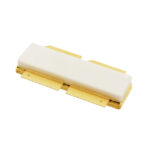 MMRF1317HSR5
The activity of extra discounts on wholesale prices is in full swing…
Please fill in your contact information and we will send you the latest wholesale price list.







