ChipApex | Global Electronic Components Supplier
SEARCH
Search Product
Search Post
— IC芯片 | 连接器 | 传感器 | 被动器件 —
Search productSearch post
— IC芯片 | 连接器 | 传感器 | 被动器件 —
Consult the customer manager about the wholesale price.
consultation hotline:86-132-6715-2157
email:[email protected]
Contact the product manager for consultation. One-stop consultation is available.
Do you want a lower wholesale price? Please send us your inquiry and we will reply immediately.
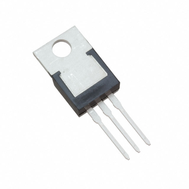
The MRF101BN is a high ruggedness N-Channel Enhancement-Mode Lateral MOSFET designed for HF and VHF communications, ISM, broadcast, and aerospace applications. It operates up to 250 MHz with a drain-source voltage of 133 Vdc and gate-source voltage range of -6.0 to +10 Vdc. The device delivers approximately 100 W CW output power at 50 Vdc across the frequency band. Key electrical characteristics include a forward transconductance of 7.1 S, input capacitance of 149 pF, and total device dissipation of 182 W at 25°C case temperature.
Verify the specific suffix BN indicates the Drain-Source-Gate pinout configuration distinct from the AN variant. Confirm RoHS compliance status directly with the manufacturer or authorized distributor documentation, as historical data may vary. Ensure the component meets current environmental regulations applicable to your region before finalizing procurement specifications.
Select the MRF101BN when a mirror pinout configuration is required for balanced push-pull circuit designs. Consider this device for wideband applications requiring operation from 1.8 MHz to 250 MHz. Evaluate thermal management requirements based on the 1.1 °C/W junction-to-case thermal resistance. Verify that the system can accommodate the specified maximum operating junction temperature of 175°C for reliable long-term performance.
This component belongs to the MRF101 series of broadband RF power LDMOS transistors manufactured by NXP Semiconductors. The series includes variants like the MRF101AN, which shares identical electrical performance but features a Gate-Source-Drain pinout. Both variants are included in the NXP product longevity program, ensuring assured supply for a minimum of 15 years after launch.
The MRF101AN serves as a functional substitute with identical electrical specifications. Designers must account for the reversed pinout configuration between the AN and BN variants during PCB layout and assembly to ensure correct connectivity.
 MRF101BN
The activity of extra discounts on wholesale prices is in full swing…
Please fill in your contact information and we will send you the latest wholesale price list.