ChipApex | Global Electronic Components Supplier
SEARCH
Search Product
Search Post
— IC芯片 | 连接器 | 传感器 | 被动器件 —
Search productSearch post
— IC芯片 | 连接器 | 传感器 | 被动器件 —
Consult the customer manager about the wholesale price.
consultation hotline:86-132-6715-2157
email:[email protected]
Contact the product manager for consultation. One-stop consultation is available.
Do you want a lower wholesale price? Please send us your inquiry and we will reply immediately.
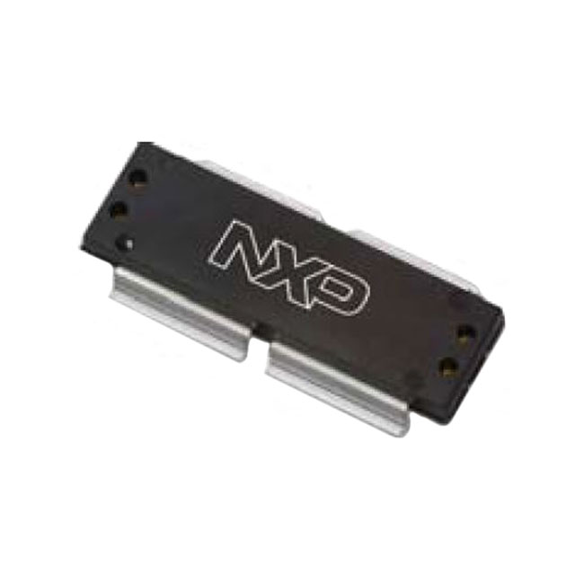
The MRF1K50GNR5 is a high ruggedness N-channel enhancement-mode lateral MOSFET designed for wideband RF power applications. It operates from 1.8 to 500 MHz with a maximum drain-source voltage of 133 Vdc and an operating voltage of 50 Vdc. The device delivers up to 1500 W CW output power at 98 MHz and 1500 W peak pulse power at 230 MHz. It features unmatched input and output designs, integrated ESD protection, and supports single-ended or push-pull configurations.
Verify the specific ordering suffix R5 confirms the tape and reel packaging format containing 50 units on a 56 mm tape width and 13-inch reel. Confirm the GN designation indicates the gull-wing lead configuration suitable for surface mount assembly. Ensure compatibility with the OM-1230G-4L plastic package dimensions and thermal requirements during procurement.
Select this component for linear applications requiring high ruggedness in high VSWR environments. It is characterized for operation from 30 to 50 V, making it versatile for various supply voltages. The device is suitable for Class C operation due to its extended negative gate-source voltage range. Consider the recommended MRFE6VS25N driver for optimal performance in common source amplifier configurations.
This part belongs to NXP's wideband RF power LDMOS transistor family, specifically engineered for industrial and broadcast sectors. The MRF1K50GN variant shares core electrical characteristics with the MRF1K50N but differs in package termination style. It is designed to withstand extreme load mismatches without degradation, ensuring reliability in demanding aerospace and mobile radio infrastructure applications.
Public confirmed substitute part numbers are not available in the provided documentation.
The maximum drain-source voltage (VDSS) rating is -0.5 to +133 Vdc.
Yes, the device can be used in either single-ended or push-pull configurations.
The typical power gain (Gps) at 98 MHz is 23.1 dB under continuous wave conditions.
 MRF1K50GNR5
The activity of extra discounts on wholesale prices is in full swing…
Please fill in your contact information and we will send you the latest wholesale price list.