 ChipApex | Global Electronic Components Supplier
SEARCH
Search Product
Search Post
— IC芯片 | 连接器 | 传感器 | 被动器件 —
Search productSearch post
— IC芯片 | 连接器 | 传感器 | 被动器件 —
Consult the customer manager about the wholesale price.
consultation hotline:86-132-6715-2157
email:[email protected]
Contact the product manager for consultation. One-stop consultation is available.
Do you want a lower wholesale price? Please send us your inquiry and we will reply immediately.
The MRF6S18100NR1 is an N-Channel Enhancement-Mode Lateral MOSFET designed for GSM and GSM EDGE base station applications operating between 1805 MHz and 1990 MHz. It delivers 100 Watts output power at 28 Volts with a typical gain of 14.5 dB and drain efficiency of 49%. For GSM EDGE, it provides 40 Watts average power with 15 dB gain and 35% efficiency. The device features integrated ESD protection, internal matching, and qualified operation up to 32 Vdc.
Verify the specific package style required for the application, as the NR1 suffix corresponds to the TO-270WB-4 case outline. Confirm that the component meets RoHS compliance standards if mandated by the project specifications. Ensure the procurement channel sources from authorized distributors to guarantee authenticity and traceability of the semiconductor material.
Select this component for high-power linear amplification in cellular infrastructure requiring robust thermal performance. The device supports junction temperatures up to 225°C, allowing for higher power density designs compared to standard plastic packages. Evaluate the internal matching against external network requirements to optimize system footprint and insertion loss within the target frequency band.
This part belongs to the MRF6S18100N series of RF power lateral MOSFETs manufactured by Freescale Semiconductor, now NXP USA Inc. The series targets the 1800 MHz to 2000 MHz spectrum for wireless communication infrastructure. The NR1 variant specifically denotes the tape and reel packaging configuration suitable for automated surface-mount assembly processes.
MRF6S18100NBR1
The maximum operating junction temperature is 225°C.
Yes, the device is internally matched on both the input and output ports.
Yes, it is capable of handling 5:1 VSWR at 28 Vdc and 100 Watts CW output power.
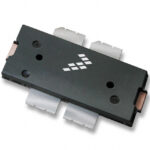 MRF6S18100NR1
The activity of extra discounts on wholesale prices is in full swing…
Please fill in your contact information and we will send you the latest wholesale price list.







