ChipApex | Global Electronic Components Supplier
SEARCH
Search Product
Search Post
— IC芯片 | 连接器 | 传感器 | 被动器件 —
Search productSearch post
— IC芯片 | 连接器 | 传感器 | 被动器件 —
Consult the customer manager about the wholesale price.
consultation hotline:86-132-6715-2157
email:[email protected]
Contact the product manager for consultation. One-stop consultation is available.
Do you want a lower wholesale price? Please send us your inquiry and we will reply immediately.
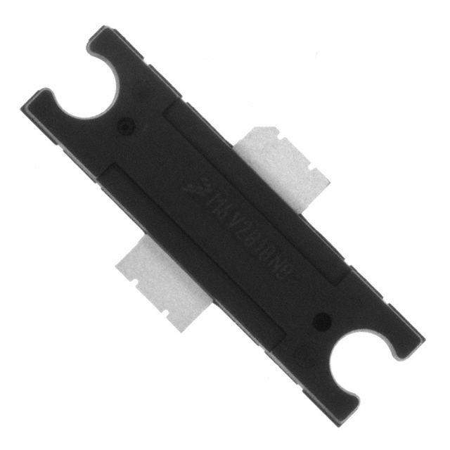
The MRF6S9060NBR1 is an N-Channel Enhancement-Mode Lateral MOSFET designed for broadband commercial and industrial applications up to 1000 MHz. It operates at a drain-source voltage of 68 Vdc with a maximum junction temperature of 225°C. Typical performance includes 14 Watts average output power in single-carrier N-CDMA at 880 MHz, 21 Watts average in GSM EDGE across 921-960 MHz, and 60 Watts continuous wave output in GSM applications.
Verify component authenticity through authorized channels as the device is no longer manufactured. Confirm RoHS compliance status via Certificate of Analysis. Validate package integrity against specified thermal resistance values before integration into final assemblies.
Evaluate thermal management requirements carefully due to the 225°C maximum junction temperature capability. Ensure biasing circuits support the specified gate threshold voltage range. Verify that the application environment remains within the defined operating case temperature limits to maintain reliability.
This lateral N-channel RF power MOSFET was originally produced by Freescale Semiconductor. The manufacturing line has since transitioned to NXP Semiconductors following corporate restructuring. The specific B suffix variant indicates a lead-free termination configuration compliant with environmental directives.
Refer to Device Migration notification PCN12895 for details regarding the replacement of this component by the MRFE6S9060NR1.
 MRF6S9060NBR1
The activity of extra discounts on wholesale prices is in full swing…
Please fill in your contact information and we will send you the latest wholesale price list.