ChipApex | Global Electronic Components Supplier
SEARCH
Search Product
Search Post
— IC芯片 | 连接器 | 传感器 | 被动器件 —
Search productSearch post
— IC芯片 | 连接器 | 传感器 | 被动器件 —
Consult the customer manager about the wholesale price.
consultation hotline:86-132-6715-2157
email:[email protected]
Contact the product manager for consultation. One-stop consultation is available.
Do you want a lower wholesale price? Please send us your inquiry and we will reply immediately.
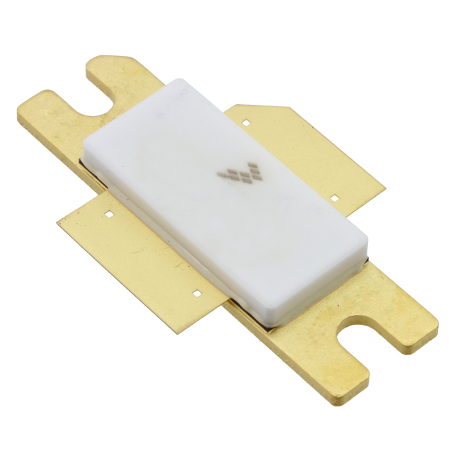
The MRF6S9130HR3 is an N-Channel Enhancement-Mode Lateral MOSFET designed for base station applications in the 865 to 960 MHz frequency range. It operates at a drain-source voltage of 28 Vdc with a maximum rating of 68 Vdc. The device delivers 27 Watts average output power for single-carrier N-CDMA signals at 880 MHz, achieving a power gain of 19.2 dB and a drain efficiency of 30.5%. For GSM EDGE applications within the 921-960 MHz band, it provides 56 Watts average output power with 44% drain efficiency. The component utilizes an NI-780 package.
Verify the specific ordering suffix against current manufacturer documentation before procurement. Confirm that the R3 suffix corresponds to the required tape and reel packaging configuration. Ensure compatibility with the NI-780 case style. Validate RoHS compliance status as specified in the official datasheet prior to finalizing supply chain arrangements.
Select this component for designs requiring high ruggedness and internal matching within the 865 to 960 MHz spectrum. Evaluate thermal management requirements based on the junction-to-case thermal resistance values provided in the datasheet. Consider the device's capability to handle high voltage standing wave ratios when designing output matching networks for robust system performance.
This part belongs to the RF Power Field Effect Transistors category manufactured by Freescale Semiconductor, which was later acquired by NXP USA Inc. The MRF6S9130H series represents lateral N-channel devices specifically engineered for wireless communication infrastructure. These transistors are characterized for use in demanding linear amplifier environments requiring high power density.
Public confirmed substitute part numbers: MRFE6S9130HR3, MRFE6S9130HSR3. Refer to Device Migration PCN12895 for detailed transition information.
 MRF6S9130HR3
The activity of extra discounts on wholesale prices is in full swing…
Please fill in your contact information and we will send you the latest wholesale price list.