 ChipApex | Global Electronic Components Supplier
SEARCH
Search Product
Search Post
— IC芯片 | 连接器 | 传感器 | 被动器件 —
Search productSearch post
— IC芯片 | 连接器 | 传感器 | 被动器件 —
Consult the customer manager about the wholesale price.
consultation hotline:86-132-6715-2157
email:[email protected]
Contact the product manager for consultation. One-stop consultation is available.
Do you want a lower wholesale price? Please send us your inquiry and we will reply immediately.
The MRF6V2010NR1 is an N-Channel Enhancement-Mode Lateral MOSFET designed for CW large-signal output and driver applications up to 450 MHz. It operates at a maximum drain-source voltage of 50 Vdc with a typical power gain of 23.9 dB and drain efficiency of 62% at 220 MHz, delivering 10 W CW output power. The device features integrated ESD protection and is qualified for operation up to 225°C junction temperature.
Verify the R1 suffix indicates a 500-unit reel quantity on a 24 mm tape width. Confirm the TO-270-2 plastic package matches the design requirements. Ensure compliance with RoHS standards as specified in the ordering information table.
Select this component for broadband RF applications requiring high reliability under continuous wave conditions. Consider the 225°C operating junction temperature for thermal management. Verify impedance matching networks against the provided series equivalent source and load impedances for optimal performance.
This part belongs to the MRF6V2010N family, which includes variants like MRF6V2010NB and MRF6V2010GN. These lateral N-channel MOSFETs are engineered for robust RF power amplification across a wide frequency range, supporting various mounting methods including bolt-down and solder reflow.
MRF6V2010N
The maximum operating junction temperature is 225°C.
Yes, the MRF6V2010NR1 features integrated ESD protection characterized according to Human Body Model, Machine Model, and Charge Device Model standards.
At 220 MHz with a 50 Vdc supply and 10 W CW output power, the typical power gain is 23.9 dB.
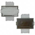 MRF6V2010NR1
The activity of extra discounts on wholesale prices is in full swing…
Please fill in your contact information and we will send you the latest wholesale price list.





