 ChipApex | Global Electronic Components Supplier
SEARCH
Search Product
Search Post
— IC芯片 | 连接器 | 传感器 | 被动器件 —
Search productSearch post
— IC芯片 | 连接器 | 传感器 | 被动器件 —
Consult the customer manager about the wholesale price.
consultation hotline:86-132-6715-2157
email:[email protected]
Contact the product manager for consultation. One-stop consultation is available.
Do you want a lower wholesale price? Please send us your inquiry and we will reply immediately.
The ART2K0FESU is a dual N-channel LDMOS RF power transistor based on Advanced Rugged Technology (ART). It operates within a frequency range of 1 MHz to 400 MHz and supports a maximum drain-source voltage of 65 V. The device delivers up to 2000 W output power with a typical gain of 28.4 dB at 108 MHz. Key electrical parameters include a drain-source breakdown voltage of 203 V, an on-state resistance of 0.100 Ω, and a gate-source threshold voltage of 2.5 V. It features integrated dual-sided ESD protection and is housed in a SOT539BN earless flanged balanced ceramic package.
Verify the specific ordering suffix 'U' corresponds to the SOT539BN package variant when sourcing. Confirm RoHS compliance status via official Ampleon product details pages prior to procurement. Ensure handling procedures adhere to ESD sensitivity classifications C2A and HBM Class 2 to prevent device damage during assembly and testing.
Select this component for broadband RF applications requiring high power density and robustness against load mismatches. The dual-section design facilitates push-pull configurations for improved efficiency and thermal management. Verify that the operating voltage remains within the characterized 30 V to 65 V range to ensure optimal performance and longevity.
The ART2K0FESU belongs to the ART2K0FE family of power LDMOS transistors manufactured by Ampleon. This series utilizes Advanced Rugged Technology derived from the company's ninth-generation high-voltage LDMOS process. The family includes variants with different packaging options, such as SOT539AN and SOT1248C, tailored for various mounting and thermal requirements.
Direct replacements within the same family include ART2K0FEU (SOT539AN) and ART2K0FEGJ (SOT1248C). Substitution requires verification of package compatibility and pinout alignment. Ensure that the alternative package meets the thermal resistance and mechanical mounting specifications of the original design.
The ART2K0FESU can withstand a load mismatch corresponding to a VSWR greater than or equal to 65:1 through all phases under specified pulsed RF conditions.
Yes, the transistor features integrated dual-sided ESD protection, which enables Class C operation and allows for complete switch-off of the device.
The typical thermal resistance from junction to case (Rth(j-c)) is 0.077 K/W, measured at a junction temperature of 95 °C under RF conditions.
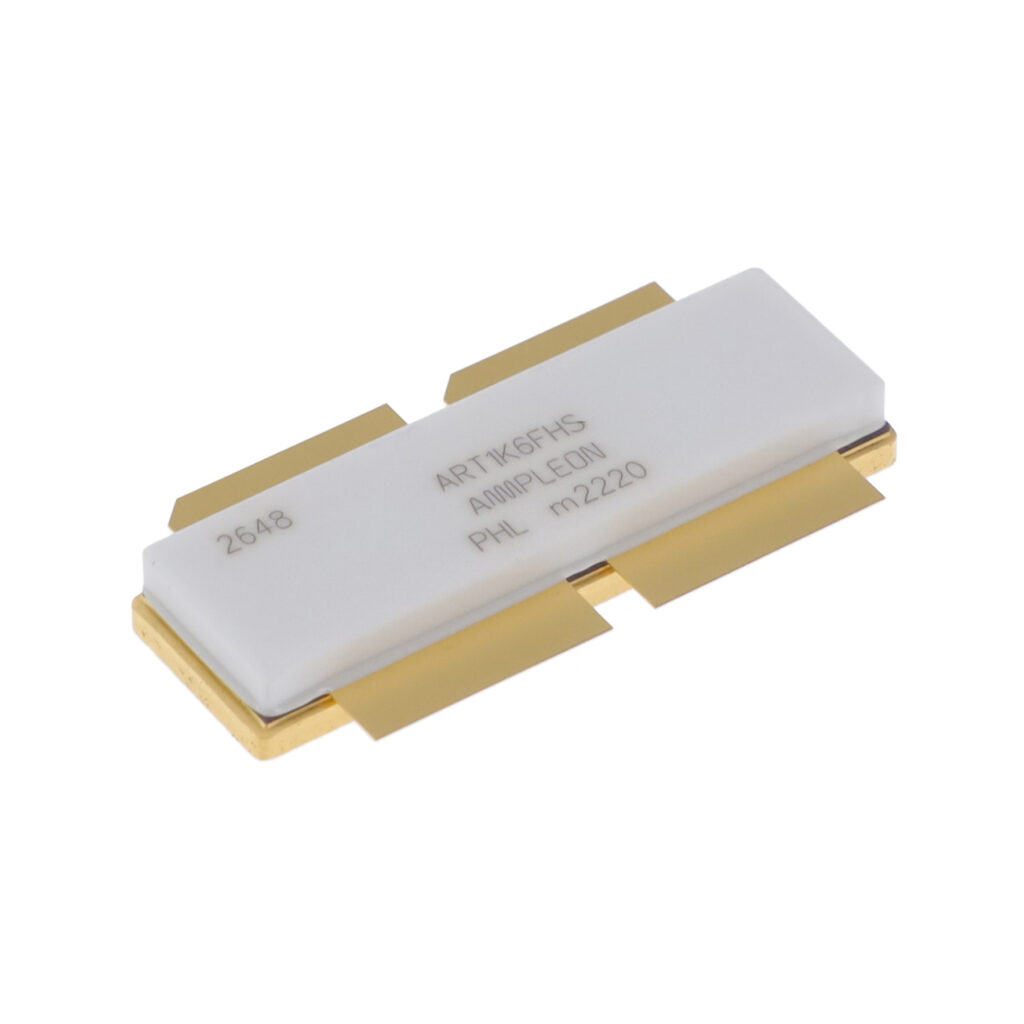

 ART2K0FESU
The activity of extra discounts on wholesale prices is in full swing…
Please fill in your contact information and we will send you the latest wholesale price list.



