ChipApex | Global Electronic Components Supplier
SEARCH
Search Product
Search Post
— IC芯片 | 连接器 | 传感器 | 被动器件 —
Search productSearch post
— IC芯片 | 连接器 | 传感器 | 被动器件 —
Consult the customer manager about the wholesale price.
consultation hotline:86-132-6715-2157
email:[email protected]
Contact the product manager for consultation. One-stop consultation is available.
Do you want a lower wholesale price? Please send us your inquiry and we will reply immediately.
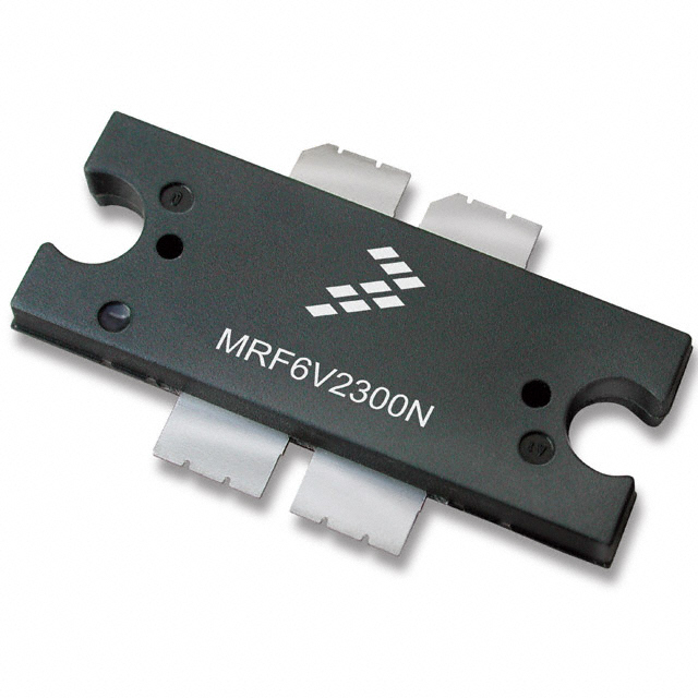
The MRF6V4300NBR1 is an N-Channel Enhancement-Mode Lateral MOSFET designed for CW large-signal output and driver applications up to 600 MHz. It operates at a maximum drain-source voltage of 110 Vdc and delivers 300 Watts output power at 450 MHz with 22 dB gain and 60% efficiency. The device features integrated ESD protection, a 225°C capable plastic package, and RoHS compliance.
Verify the exact ordering suffix against official documentation to confirm packaging specifications. Confirm that the component meets all required environmental standards and regulatory certifications before finalizing procurement decisions.
Evaluate thermal management requirements carefully due to high power dissipation. Ensure the design supports the specified operating junction temperature limits. Verify impedance matching networks align with the provided series equivalent parameters for optimal performance.
This component belongs to the MRF6V4300N family of broadband RF power lateral MOSFETs. It is engineered for single-ended configurations in industrial, medical, and scientific equipment requiring reliable high-power amplification across wide frequency bands.
Consult official manufacturer documentation for confirmed substitute part numbers. Do not assume cross-compatibility without verifying electrical characteristics and pinout configurations.
The maximum operating junction temperature is 225°C.
Yes, it features a greater negative gate-source voltage range specifically designed to improve Class C operation.
The exposed backside of the package serves as the source terminal for the transistor.
 MRF6V4300NBR1
The activity of extra discounts on wholesale prices is in full swing…
Please fill in your contact information and we will send you the latest wholesale price list.