ChipApex | Global Electronic Components Supplier
SEARCH
Search Product
Search Post
— IC芯片 | 连接器 | 传感器 | 被动器件 —
Search productSearch post
— IC芯片 | 连接器 | 传感器 | 被动器件 —
Consult the customer manager about the wholesale price.
consultation hotline:86-132-6715-2157
email:[email protected]
Contact the product manager for consultation. One-stop consultation is available.
Do you want a lower wholesale price? Please send us your inquiry and we will reply immediately.
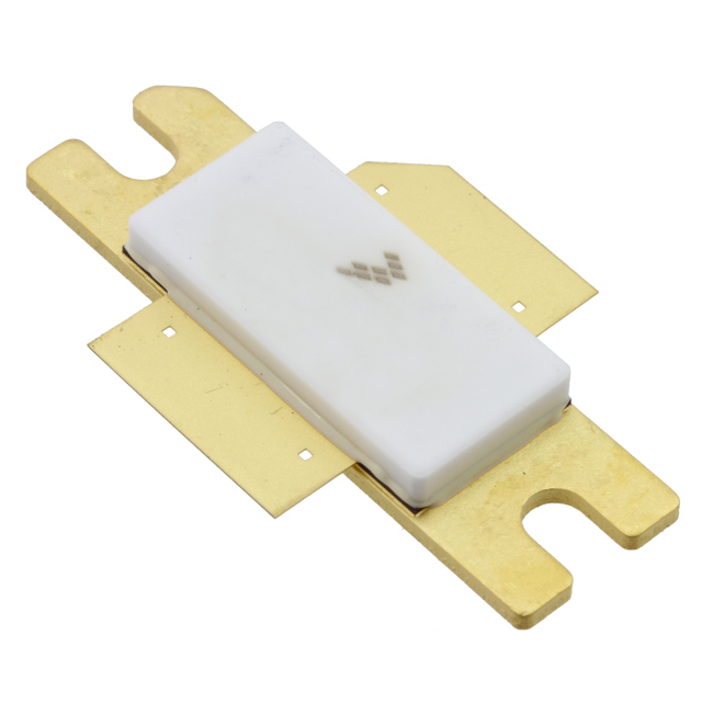
The MRF7S18125AHR5 is an N-channel enhancement-mode lateral MOSFET designed for GSM and GSM EDGE base station applications operating between 1800 MHz and 2000 MHz. It supports Class AB and Class C modulation schemes. Typical performance at VDD = 28 Volts, IDQ = 1100 mA, and f = 1880 MHz includes a power gain of 17 dB and drain efficiency of 55% with 125 Watts CW output. For GSM EDGE, it delivers 57 Watts average output with 38% efficiency and 1.75% rms EVM. The device features internal input and output matching networks.
Verify the specific ordering suffix to confirm the reel packaging format. The R3 suffix indicates units are supplied in a 56 mm, 13-inch tape and reel containing 250 units. Ensure the component matches the required package style (Case 465-06 or Case 465A-06) for your PCB layout. Confirm RoHS compliance status during procurement.
Select this component for wideband RF power amplification within the 1805 MHz to 1880 MHz frequency range. It requires a 28 Vdc supply voltage and is optimized for high linearity and efficiency in digital cellular environments. Designers must account for its thermal characteristics, specifically the junction-to-case resistance, to maintain safe operating temperatures under continuous wave conditions.
This part belongs to the Freescale Semiconductor (now NXP) LDMOS family, originally developed for wireless infrastructure. It utilizes advanced lateral MOSFET technology to deliver high power density. The device was engineered to replace older discrete transistor solutions by integrating matching networks directly onto the die, simplifying amplifier design and reducing board space requirements.
MRF7S18125AHSR3
The maximum operating junction temperature is 225 °C.
No, the device is internally matched on both the input and output sides for ease of use.
The typical drain efficiency is 55% when operating at 125 Watts CW with a 28 Volt supply.
 MRF7S18125AHR5
The activity of extra discounts on wholesale prices is in full swing…
Please fill in your contact information and we will send you the latest wholesale price list.