 ChipApex | Global Electronic Components Supplier
SEARCH
Search Product
Search Post
— IC芯片 | 连接器 | 传感器 | 被动器件 —
Search productSearch post
— IC芯片 | 连接器 | 传感器 | 被动器件 —
Consult the customer manager about the wholesale price.
consultation hotline:86-132-6715-2157
email:[email protected]
Contact the product manager for consultation. One-stop consultation is available.
Do you want a lower wholesale price? Please send us your inquiry and we will reply immediately.
The MRF7S18125BHSR5 is an N-channel enhancement-mode lateral MOSFET designed for GSM and GSM EDGE base station applications operating between 1800 MHz and 2000 MHz. It supports Class AB and Class C modulations with a typical drain efficiency of 55% at 125 Watts CW output power (1930 MHz). The device features integrated ESD protection, internal matching networks, and RoHS compliance. Maximum ratings include a drain-source voltage of 65 Vdc, gate-source voltage limits from -6.0 to +10 Vdc, and an operating junction temperature up to 225 °C.
Verify the specific ordering suffix against official documentation to confirm packaging details. The datasheet indicates that the R3 suffix corresponds to tape and reel packaging containing 250 units per 56 mm reel. Ensure compatibility with the required thermal management solutions, as continuous operation at maximum temperatures affects mean time to failure. Confirm RoHS compliance status through the manufacturer's material declaration before finalizing procurement specifications.
Select this component for designs requiring high linearity and efficiency in the 1800-2000 MHz band. The internal matching reduces external component count but requires adherence to specified test fixture impedances. Evaluate thermal resistance characteristics carefully, as junction-to-case resistance varies significantly based on output power levels. Validate performance under actual load pull conditions rather than relying solely on standard 50-ohm system data.
This device belongs to the Freescale Semiconductor RF Power Field Effect Transistor family, specifically engineered for wireless communication infrastructure. Originally developed by Freescale Semiconductor, these lateral MOSFETs are optimized for robust performance in demanding cellular environments. The product line emphasizes reliability and ease of use through integrated protection and matching features tailored for base station architectures.
Consult official cross-reference lists or contact the manufacturer directly for verified substitute part numbers. Do not assume functional equivalence with other models in the series without reviewing specific electrical parameter deviations and pinout configurations.
The typical drain efficiency is 55% when operating at 28 Volts, 1100 mA quiescent current, and 1930 MHz.
The MRF7S18125BHSR5 includes integrated ESD protection characterized to meet minimum Human Body Model Class 1B, Machine Model Class A, and Charge Device Model Class IV standards.
Yes, the transistor is internally matched on both the input and output sides to facilitate easier circuit design and implementation.
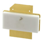 MRF7S18125BHSR5
The activity of extra discounts on wholesale prices is in full swing…
Please fill in your contact information and we will send you the latest wholesale price list.





