ChipApex | Global Electronic Components Supplier
SEARCH
Search Product
Search Post
— IC芯片 | 连接器 | 传感器 | 被动器件 —
Search productSearch post
— IC芯片 | 连接器 | 传感器 | 被动器件 —
Consult the customer manager about the wholesale price.
consultation hotline:86-132-6715-2157
email:[email protected]
Contact the product manager for consultation. One-stop consultation is available.
Do you want a lower wholesale price? Please send us your inquiry and we will reply immediately.
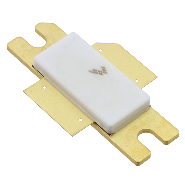
The MRF8S18120HR5 is an N-Channel Enhancement-Mode Lateral MOSFET designed for GSM and GSM EDGE base station applications operating between 1805 MHz and 1880 MHz. It supports Class AB and Class C operations with a drain-source voltage of 65 Vdc and an operating voltage of 32 Vdc. The device delivers 72 Watts CW output power at 28 Vdc, achieving up to 53.9% drain efficiency. It handles 120 Watts CW at the 1 dB compression point and withstands 150 Watts CW under overdrive conditions.
Verify the specific suffix against official documentation to confirm packaging details. Confirm RoHS compliance status through current manufacturer declarations. Ensure the component matches the NI-780 package style required for the intended circuit layout. Validate thermal resistance specifications against the actual mounting conditions used in the final assembly design.
Select this component for wideband RF power applications requiring high linearity and efficiency within the 1805 to 1880 MHz frequency range. Consider the internal matching network to simplify impedance transformation requirements. Evaluate the thermal management capabilities based on the specified junction-to-case resistance values. Verify compatibility with standard 50 ohm system test fixtures during the design phase.
This part belongs to the Freescale Semiconductor RF Power Field Effect Transistors family. It utilizes lateral metal-on-silicon technology optimized for cellular infrastructure. The device is housed in the NI-780 case style. It serves as a discrete solution for high-power radio frequency amplification tasks.
Consult official datasheets for direct substitutes such as the MRF8S18120H variants. Verify pinout and thermal characteristics before implementation.
 MRF8S18120HR5
The activity of extra discounts on wholesale prices is in full swing…
Please fill in your contact information and we will send you the latest wholesale price list.