ChipApex | Global Electronic Components Supplier
SEARCH
Search Product
Search Post
— IC芯片 | 连接器 | 传感器 | 被动器件 —
Search productSearch post
— IC芯片 | 连接器 | 传感器 | 被动器件 —
Consult the customer manager about the wholesale price.
consultation hotline:86-132-6715-2157
email:[email protected]
Contact the product manager for consultation. One-stop consultation is available.
Do you want a lower wholesale price? Please send us your inquiry and we will reply immediately.
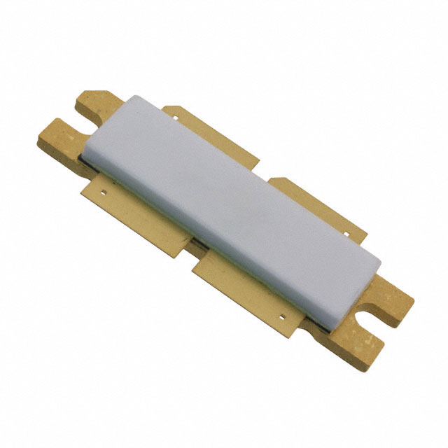
The MRFE6VP61K25HR5 is a high ruggedness N-channel enhancement-mode lateral MOSFET designed for wideband RF power applications. It operates across a frequency range of 1.8 to 600 MHz with a maximum drain-source voltage of 133 Vdc and a total device dissipation of 1333 W at 25°C case temperature. The transistor delivers up to 1250 W continuous wave output power at 50 Vdd, characterized by a typical power gain of 24.0 dB and drain efficiency of 74.0% at 230 MHz under pulsed conditions. It features unmatched input and output designs suitable for single-ended or push-pull configurations.
Verify the specific suffix HR5 against the official datasheet to confirm tape and reel packaging specifications. Confirm that the ordering part number matches the exact electrical characteristics required for the target application. Ensure compatibility with the NI-1230H-4S package dimensions for proper thermal management and mechanical integration into the final assembly.
Select this component when designing wideband amplifiers operating between 1.8 and 600 MHz that require high power density. Consider its suitability for linear modes where appropriate biasing is applied. Evaluate the thermal resistance characteristics to ensure adequate heat sinking for continuous wave operations. Verify that the system can support the required gate-source voltage thresholds for optimal performance.
This device belongs to the MRFE6VP61K25 series of RF Power LDMOS Transistors manufactured by Freescale Semiconductor, now NXP Semiconductors. The series includes variants such as MRFE6VP61K25HR6, MRFE6VP61K25HSR5, and MRFE6VP61K25GSR5, which share similar electrical profiles but differ in packaging and shipping formats. These transistors are engineered for high-power, high-efficiency RF amplification in challenging electromagnetic environments.
MRFE6VP61K25HR6
The maximum drain-source voltage (VDSS) rating is -0.5 to +133 Vdc.
Yes, the device is designed to be used in either single-ended or push-pull configurations due to its unmatched input and output design.
The typical power gain (Gps) is 24.0 dB at 230 MHz under pulsed conditions with VDD = 50 Volts and IDQ = 100 mA.
 MRFE6VP61K25HR5
The activity of extra discounts on wholesale prices is in full swing…
Please fill in your contact information and we will send you the latest wholesale price list.