ChipApex | Global Electronic Components Supplier
SEARCH
Search Product
Search Post
— IC芯片 | 连接器 | 传感器 | 被动器件 —
Search productSearch post
— IC芯片 | 连接器 | 传感器 | 被动器件 —
Consult the customer manager about the wholesale price.
consultation hotline:86-132-6715-2157
email:[email protected]
Contact the product manager for consultation. One-stop consultation is available.
Do you want a lower wholesale price? Please send us your inquiry and we will reply immediately.
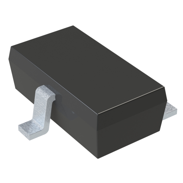
The MSC2295-CT1 is a high-voltage power MOSFET manufactured by onsemi, designed for demanding industrial and automotive applications. It features an N-channel configuration with a drain-source voltage rating of 950 V. The device exhibits a maximum on-resistance of 2.29 Ω at a gate-source voltage of 10 V. It is housed in a compact TO-263 (D2PAK) surface-mount package, facilitating efficient thermal management and PCB integration. The component operates within a junction temperature range of -55 °C to 175 °C, ensuring reliability under extreme conditions. Key electrical parameters include a continuous drain current of 1.8 A and a pulsed drain current capability of 7.2 A, supporting robust performance in high-efficiency switching converters.
Verify the specific suffix CT1 against the manufacturer's official datasheet to confirm tape-and-reel packaging specifications and quantity per reel. Ensure that the ordering part number matches the exact voltage and resistance grades required for your design. Cross-reference with authorized distributors to confirm current availability and lead times, as production status may vary. Request sample units for initial prototyping and thermal testing before committing to volume orders.
Select this component when a 950 V rating is necessary for high-voltage bus applications. The 2.29 Ω RDS(on) offers a balance between conduction losses and cost for moderate current levels around 1.8 A. Consider the TO-263 package for its thermal performance compared to smaller packages. Evaluate the gate charge requirements against your driver capabilities to ensure adequate switching speeds without excessive drive power loss.
This device belongs to onsemi's portfolio of high-voltage power MOSFETs, often utilizing advanced trench technology for superior performance. It complements lower-voltage options in hybrid systems where high isolation is required. The product line targets industries requiring high reliability and efficiency, such as renewable energy inverters and electric vehicle charging infrastructure. Its design aligns with industry standards for thermal and electrical robustness in harsh environments.
When substituting, verify that the replacement part meets or exceeds the 950 V drain-source voltage and 2.29 Ω maximum on-resistance. Ensure the pinout compatibility with the TO-263 package to avoid PCB redesign. Check that the gate charge and threshold voltage are similar to maintain existing driver performance. Confirm that the new component holds equivalent automotive or industrial qualification certifications if required by the application.
 MSC2295-CT1
The activity of extra discounts on wholesale prices is in full swing…
Please fill in your contact information and we will send you the latest wholesale price list.