ChipApex | Global Electronic Components Supplier

SEARCH
Search Product
Search Post
— IC芯片 | 连接器 | 传感器 | 被动器件 —
Search productSearch post
— IC芯片 | 连接器 | 传感器 | 被动器件 —
Consult the customer manager about the wholesale price.
consultation hotline:86-132-6715-2157
email:[email protected]
Contact the product manager for consultation. One-stop consultation is available.
Do you want a lower wholesale price? Please send us your inquiry and we will reply immediately.
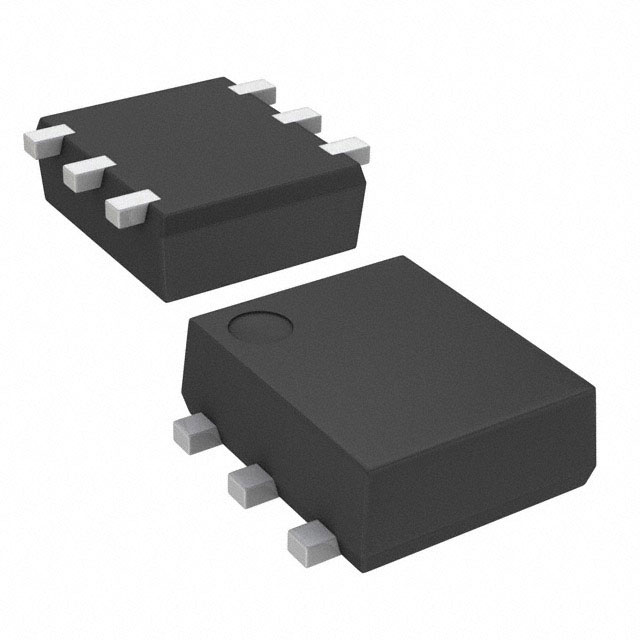
MTM763250LBF is listed in the FET, MOSFET Arrays range at ChipApex. The manufacturer field lists Panasonic Electronic Components. Its product description is MOSFET N/P-CH 20V 1.7A WSMINI6. Review the specifications below when checking this part for your BOM.
The MTM763250LBF is a dual MOSFET component containing one N-channel and one P-channel silicon field-effect transistor in a single WSMini6-F1-B (SC-113DA) package. The N-channel device features a drain-source voltage of 20 V, a continuous drain current of 1.7 A, and a typical on-resistance of 95 mΩ at VGS = 4.0 V. The P-channel device offers a drain-source voltage of -20 V, a continuous drain current of 2.1 A, and a typical on-resistance of 300 mΩ at VGS = -4.0 V. Total power dissipation is rated at 700 mW on a ceramic substrate.
Verify the manufacturer designation carefully, as the semiconductor business was transferred from Panasonic Corporation to Nuvoton Technology Corporation Japan in September 2020. Ensure that the specific ordering suffix matches the required packaging configuration, such as embossed tape and reel quantities, before finalizing procurement orders.
Select this component when a compact solution requiring both N-channel and P-channel logic-level switching is necessary. Verify that the operating gate-source voltage aligns with the specified thresholds for optimal on-resistance performance. Confirm thermal management capabilities against the absolute maximum ratings for total power dissipation.
This component belongs to the basic part number series of individual N-channel and P-channel MOSFETs rated for 20 V operation. It is designed for general-purpose switching applications within the broader portfolio of discrete semiconductor devices manufactured by Nuvoton Technology Corporation Japan.
Consult official substitution lists or datasheets for equivalent dual MOSFET packages. Verify pin compatibility and electrical parameters before replacing the original component in existing designs.
The component utilizes the WSMini6-F1-B package, also designated as SC-113DA.
Pin 1 is Source FET1, Pin 2 is Gate FET1, Pin 3 is Drain FET2, Pin 4 is Source FET2, Pin 5 is Gate FET2, and Pin 6 is Drain FET1.
The peak drain current for the N-channel device is 3.0 A under pulse conditions with a duty cycle of 1% or less.
Explore related parts through FETs, MOSFETs, Transistors, Discrete Semiconductor Products, all product categories.
 MTM763250LBF

The activity of extra discounts on wholesale prices is in full swing…
Please fill in your contact information and we will send you the latest wholesale price list.