ChipApex | Global Electronic Components Supplier
SEARCH
Search Product
Search Post
— IC芯片 | 连接器 | 传感器 | 被动器件 —
Search productSearch post
— IC芯片 | 连接器 | 传感器 | 被动器件 —
Consult the customer manager about the wholesale price.
consultation hotline:86-132-6715-2157
email:[email protected]
Contact the product manager for consultation. One-stop consultation is available.
Do you want a lower wholesale price? Please send us your inquiry and we will reply immediately.
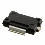
The MW6S010GNR1 is an N-channel enhancement-mode lateral MOSFET RF power device designed for base station applications up to 1500 MHz. It operates at a drain-source voltage of 28 Vdc with a maximum rating of 68 Vdc and supports junction temperatures up to 225°C. The component delivers 10 W PEP output power, achieving 18 dB power gain and 32% drain efficiency at 960 MHz. It features integrated ESD protection and on-chip RF feedback for broadband stability.
Verify the specific ordering suffix 'GNR1' against current manufacturer documentation to confirm package style and reel specifications. Confirm RoHS compliance status and moisture sensitivity level ratings prior to assembly planning. Ensure thermal management solutions support the specified 225°C junction temperature capability.
Select this component for designs requiring high linearity and broadband performance in the 450-1500 MHz range. Evaluate impedance matching networks using the provided series equivalent large-signal impedance parameters. Consider the TO-270-2 gull-wing plastic package constraints for PCB layout and mounting requirements.
This part belongs to the Freescale Semiconductor RF Power Field Effect Transistor family, specifically the MW6S010N series. It is manufactured by NXP USA Inc., following the acquisition of Freescale. The device is characterized for use in wireless communication infrastructure where robust RF performance and thermal resilience are critical.
Consult official substitution lists for compatible lateral N-channel MOSFETs within the same power class. Verify pinout compatibility and thermal resistance characteristics when considering alternative packages or manufacturers.
The maximum operating junction temperature is 225°C.
Yes, the device includes integrated ESD protection and on-chip RF feedback for stability.
The typical power gain is 18 dB at 960 MHz under standard test conditions.
 MW6S010GNR1
The activity of extra discounts on wholesale prices is in full swing…
Please fill in your contact information and we will send you the latest wholesale price list.