 ChipApex | Global Electronic Components Supplier

SEARCH
Search Product
Search Post
— IC芯片 | 连接器 | 传感器 | 被动器件 —
Search productSearch post
— IC芯片 | 连接器 | 传感器 | 被动器件 —
Consult the customer manager about the wholesale price.
consultation hotline:86-132-6715-2157
email:[email protected]
Contact the product manager for consultation. One-stop consultation is available.
Do you want a lower wholesale price? Please send us your inquiry and we will reply immediately.
N74F299N,602 is listed in the Shift Registers range at ChipApex. The manufacturer field lists NXP USA Inc.. Its product description is IC SHIFT REGISTER 8BIT 20DIP. Review the specifications below when checking this part for your BOM.
The N74F299N,602 is an 8-bit universal shift/storage register with 3-State outputs manufactured by NXP USA Inc. It operates within a supply voltage range of 4.5V to 5.5V and supports a commercial temperature range of 0°C to +70°C. The device features four operating modes: hold, shift left, shift right, and parallel load. It includes serial inputs for expansion and separate outputs for Q0 and Q7. The maximum clock frequency is 115 MHz at typical conditions. Total supply current is typically 58 mA.
Verify the specific ordering code matches the required package type, as the N74F299N,602 designation corresponds to the 20-pin plastic DIP (SOT146-1). Confirm that the component status aligns with project lifecycle requirements, noting that older Philips/NXP logic families may have varying availability or obsolescence statuses across different distributors. Ensure compatibility with existing board layouts regarding the DIP-20 footprint.
Select this component when an 8-bit universal shift register with tri-state outputs is required in a through-hole DIP package. Consider the 74F logic family speed characteristics and power consumption profile relative to system needs. Verify that the input loading and fan-out specifications meet the driving requirements of connected circuitry. Ensure the design accommodates the separate serial I/O pins available on the package.
This part belongs to the 74F series of high-speed TTL logic devices originally developed by Philips Semiconductors and now produced by NXP. The 74F299 specifically provides versatile data handling capabilities within a standard 20-pin dual in-line package format. It serves as a foundational building block for digital systems requiring flexible data shifting and storage operations with bus-compatible outputs.
Compatible substitutes include other 74F299 variants from different manufacturers offering identical logical functionality and pinouts. Verify electrical characteristics such as propagation delay and supply current against the original datasheet specifications. Ensure the replacement part supports the same 20-pin DIP package configuration for direct physical interchangeability.
The parallel load inputs and flip-flop outputs are multiplexed to shared I/O pins to reduce the total number of package pins required.
When both S0 and S1 are HIGH, the 3-State buffers are disabled in preparation for a parallel load operation, provided the Output Enable inputs are active.
Yes, even when the 3-State buffers are disabled by HIGH signals on OE0 or OE1, internal shift, hold, load, and reset operations can still occur.
Explore related parts through Logic, Integrated Circuits (ICs), all product categories, ChipApex homepage.
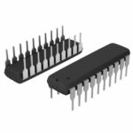 N74F299N,602

N74F299N,602 is listed in the Shift Registers range at ChipApex. The manufacturer field lists NXP USA Inc.. Its product description is IC SHIFT REGISTER…
Read More
N74F299N,602 is listed in the Shift Registers range at ChipApex. The manufacturer field lists NXP USA Inc.. Its product description is IC SHIFT REGISTER…
Read More
N74F299N,602 is listed in the Shift Registers range at ChipApex. The manufacturer field lists NXP USA Inc.. Its product description is IC SHIFT REGISTER…
Read More
Learn how a pressure transducer converts pressure into voltage, current, or digital output, and compare pressure references and key selection specs.
Read More
N74F299N,602 is listed in the Shift Registers range at ChipApex. The manufacturer field lists NXP USA Inc.. Its product description is IC SHIFT REGISTER…
Read More
N74F299N,602 is listed in the Shift Registers range at ChipApex. The manufacturer field lists NXP USA Inc.. Its product description is IC SHIFT REGISTER…
Read More
N74F299N,602 is listed in the Shift Registers range at ChipApex. The manufacturer field lists NXP USA Inc.. Its product description is IC SHIFT REGISTER…
Read More
N74F299N,602 is listed in the Shift Registers range at ChipApex. The manufacturer field lists NXP USA Inc.. Its product description is IC SHIFT REGISTER…
Read More
N74F299N,602 is listed in the Shift Registers range at ChipApex. The manufacturer field lists NXP USA Inc.. Its product description is IC SHIFT REGISTER…
Read More
N74F299N,602 is listed in the Shift Registers range at ChipApex. The manufacturer field lists NXP USA Inc.. Its product description is IC SHIFT REGISTER…
Read More
N74F299N,602 is listed in the Shift Registers range at ChipApex. The manufacturer field lists NXP USA Inc.. Its product description is IC SHIFT REGISTER…
Read More
Select MOV varistors by continuous voltage, clamping behavior, surge waveform and repetition. Check thermal disconnection, fuse coordination and replacements.
Read More
The activity of extra discounts on wholesale prices is in full swing…
Please fill in your contact information and we will send you the latest wholesale price list.





