 ChipApex | Global Electronic Components Supplier

SEARCH
Search Product
Search Post
— IC芯片 | 连接器 | 传感器 | 被动器件 —
Search productSearch post
— IC芯片 | 连接器 | 传感器 | 被动器件 —
Consult the customer manager about the wholesale price.
consultation hotline:86-132-6715-2157
email:[email protected]
Contact the product manager for consultation. One-stop consultation is available.
Do you want a lower wholesale price? Please send us your inquiry and we will reply immediately.
NDS9947 is listed in the FET, MOSFET Arrays range at ChipApex. The manufacturer field lists onsemi. Its product description is MOSFET 2P-CH 20V 3.5A 8SOIC. Review the specifications below when checking this part for your BOM.
The NDS9947 is a dual P-Channel Enhancement Mode Field Effect Transistor manufactured by onsemi. It features a Drain-Source Voltage (VDSS) of -20 V and a continuous Drain Current (ID) of ±3.5 A at 25°C. The device exhibits a maximum Static Drain-Source On-Resistance (RDS(ON)) of 0.1 Ω at VGS = -10 V and ID = -3.5 A. Total Gate Charge (Qg) is typically 19 nC. Power Dissipation (PD) for dual operation is rated at 2 W, with an Operating Temperature Range from -55 to 150 °C. The component utilizes DMOS technology in an SOIC-8 surface mount package.
Verify the manufacturer origin carefully, as Fairchild Semiconductor was acquired by onsemi. Confirm the specific ordering suffix matches the required packaging option, such as tape and reel quantities or rail configurations. Ensure the revision level aligns with your design requirements before finalizing procurement orders.
Select this component for low voltage applications where compact dual-channel integration is necessary. Evaluate thermal performance based on the specific PCB copper pad area, as junction-to-ambient resistance varies significantly with mounting surface size. Ensure gate drive voltages remain within the specified limits to maintain optimal RDS(ON) characteristics.
This component belongs to the PowerTrench series of enhancement mode field effect transistors. It represents a transition period product originally developed by Fairchild Semiconductor before the corporate acquisition by onsemi. The datasheet retains original Fairchild branding and documentation styles while being distributed under the onsemi portfolio.
NDS9948: Dual P-Channel MOSFET with higher voltage rating (-60V).
The typical total gate charge is 19 nC when tested at VDS = -10 V, ID = -3.5 A, and VGS = -10 V.
The drain-source on-resistance increases as the junction temperature rises. At TJ = 125°C, the maximum RDS(ON) increases to 0.16 Ω compared to the 0.1 Ω maximum at 25°C.
No. The manufacturer explicitly states that products are not authorized for use as critical components in life support devices without express written approval.
Explore related parts through FETs, MOSFETs, Transistors, Discrete Semiconductor Products, all product categories.
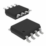 NDS9947

The activity of extra discounts on wholesale prices is in full swing…
Please fill in your contact information and we will send you the latest wholesale price list.





