ChipApex | Global Electronic Components Supplier
SEARCH
Search Product
Search Post
— IC芯片 | 连接器 | 传感器 | 被动器件 —
Search productSearch post
— IC芯片 | 连接器 | 传感器 | 被动器件 —
Consult the customer manager about the wholesale price.
consultation hotline:86-132-6715-2157
email:[email protected]
Contact the product manager for consultation. One-stop consultation is available.
Do you want a lower wholesale price? Please send us your inquiry and we will reply immediately.
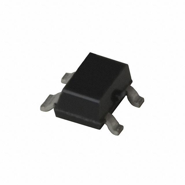
The NE34018-T1 is a GaAs Hetero-Junction FET in an SOT-343 plastic package. It operates as a low noise amplifier transistor in the 1-3 GHz range. Key electrical parameters at VDS=2V, IDS=5mA, f=2GHz include a typical Noise Figure of 0.6 dB and Associated Gain of 16.0 dB. At VDS=3V, IDS=30mA, f=2GHz, P1dB is 16.5 dBm and O/P IP3 is 32 dBm. Absolute maximum ratings are VDS=4V, VGDO/VGSO=-3V, TCH=125°C, and PT=150 mW.
Verify the specific I_DSS binning code on the reel label or datasheet orderable part number suffix. The -T1 designation indicates tape and reel packaging. Confirm the exact current range (e.g., 30-65 mA vs 60-120 mA) matches the design requirements, as performance varies significantly with bias current and device binning.
Select based on required noise figure and gain trade-offs against drain current. Higher currents increase gain and output power but raise thermal dissipation. Ensure the PCB layout supports the SOT-343 footprint and provides adequate thermal relief for the exposed source/drain pads to maintain channel temperature within the 125°C limit.
Manufactured by California Eastern Laboratories (CEL), this component is a Gallium Arsenide HJ-FET. It serves as a discrete active element for RF circuit designers requiring high linearity and low noise in compact form factors. The device is distinct from integrated MMICs, offering flexibility for custom matching networks.
Public confirmed substitute part numbers are not available in the provided documentation. Designers should consult CEL/NEC official cross-reference lists or evaluate equivalent GaAs HJ-FETs with similar SOT-343 footprints and comparable NF/Gain specifications at 2 GHz.
Pin 1 is Source, Pin 2 is Gate, Pin 3 is Source, and Pin 4 is Drain.
At VDS=2V, IDS=10mA, the typical Noise Figure increases from 0.56 dB at 900 MHz to 0.70 dB at 3000 MHz.
The absolute maximum rating for total power dissipation is 150 mW at an ambient temperature of 25°C.
 NE34018-T1
The activity of extra discounts on wholesale prices is in full swing…
Please fill in your contact information and we will send you the latest wholesale price list.