ChipApex | Global Electronic Components Supplier
SEARCH
Search Product
Search Post
— IC芯片 | 连接器 | 传感器 | 被动器件 —
Search productSearch post
— IC芯片 | 连接器 | 传感器 | 被动器件 —
Consult the customer manager about the wholesale price.
consultation hotline:86-132-6715-2157
email:[email protected]
Contact the product manager for consultation. One-stop consultation is available.
Do you want a lower wholesale price? Please send us your inquiry and we will reply immediately.
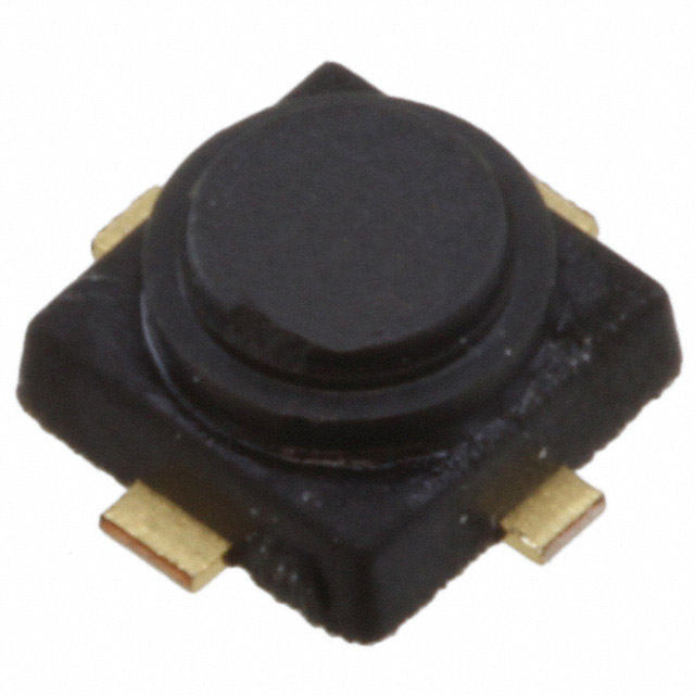
The NE3520S03 is an N-channel GaAs Heterojunction Field-Effect Transistor (HJ-FET) designed for K-band applications. It operates with a drain-to-source voltage of up to 4.0 V and a gate-to-source voltage of -3.0 V. At 20 GHz, it provides a typical noise figure of 0.65 dB and an associated gain of 13.5 dB when biased at VDS = 2 V and ID = 10 mA. The device features a saturated drain current range of 25 to 70 mA and a transconductance of 50 to 65 mS. Total power dissipation is rated at 165 mW, with a maximum channel temperature of +125 °C.
Verify the specific ordering suffix required for tape-and-reel quantity, as the base part number corresponds to sample quantities. Confirm that the CE3520K3 is accepted as a drop-in replacement if the NE3520S03 is discontinued. Ensure handling procedures account for electrostatic discharge sensitivity inherent to GaAs devices.
Select this component for designs requiring low noise performance in the K-band spectrum. Verify biasing conditions align with the recommended operating range of VDS between +1 V and +3 V. Consider the thermal constraints imposed by the 165 mW power dissipation limit and ensure the PCB layout matches the specified RF measuring pattern for accurate impedance matching.
This device belongs to the family of Gallium Arsenide HJ-FETs developed for microwave frequency operations. Manufactured originally by California Eastern Laboratories (CEL), it represents a specialized semiconductor solution for low-noise amplification in satellite and communication infrastructure. The S03 package facilitates surface-mount integration into compact RF modules.
The datasheet explicitly identifies the CE3520K3 as a drop-in replacement for the NE3520S03.
The typical noise figure is 0.65 dB when biased at VDS = 2 V and ID = 10 mA.
The absolute maximum Drain-to-Source Voltage is 4.0 V, and the Gate-to-Source Voltage is -3.0 V.
Yes, the datasheet marks the NE3520S03 as discontinued.
 NE3520S03-A
The activity of extra discounts on wholesale prices is in full swing…
Please fill in your contact information and we will send you the latest wholesale price list.