 ChipApex | Global Electronic Components Supplier

SEARCH
Search Product
Search Post
— IC芯片 | 连接器 | 传感器 | 被动器件 —
Search productSearch post
— IC芯片 | 连接器 | 传感器 | 被动器件 —
Consult the customer manager about the wholesale price.
consultation hotline:86-132-6715-2157
email:[email protected]
Contact the product manager for consultation. One-stop consultation is available.
Do you want a lower wholesale price? Please send us your inquiry and we will reply immediately.
NLVHC4094BDTR2G is listed in the Shift Registers range at ChipApex. The manufacturer field lists onsemi. Its product description is IC SHIFT REGISTER 3ST 16TSSOP. Review the specifications below when checking this part for your BOM.
The NLVHC4094BDTR2G is an automotive-grade, high-speed CMOS 8-bit serial shift and storage register manufactured by onsemi. It integrates an 8-bit shift register with a storage latch and three-state output buffers. The device operates within a DC supply voltage range of 2.0 V to 6.0 V and supports an operating temperature range from -55°C to +125°C. Data shifts on positive clock transitions, while the strobe input transfers data to the storage register. Two serial outputs facilitate cascading multiple devices.
Verify that the specific ordering suffix BDTR2G corresponds to the TSSOP-16 tape and reel packaging configuration. Confirm AEC-Q100 qualification status and PPAP capability requirements against current project specifications. Ensure compatibility with the specified 2.0 V to 6.0 V operating voltage range and -55°C to +125°C temperature limits during component selection.
Select this component when automotive reliability standards such as AEC-Q100 are mandatory. The TSSOP-16 package suits space-constrained designs requiring surface-mount assembly. Verify that the logic family voltage levels align with system interfaces. Consider the device's propagation delay characteristics relative to the maximum clock frequency requirements of the application circuit.
This part belongs to the MC74HC4094A product family, which includes standard commercial variants alongside the automotive-specific NLV prefix versions. The NLV designation indicates unique site and control change requirements distinct from non-automotive counterparts. The device functions as a fundamental building block for digital data handling in robust electronic systems.
Consult the datasheet discontinuation notice for alternative recommendations. Verify pinout and electrical parameter compatibility before substituting with other 8-bit shift registers.
The Strobe input transfers the data stored in the shift register to the storage register when set high.
Setting the OE input high enables the three-state output buffers, allowing parallel data access at the QP pins.
Explore related parts through Logic, Integrated Circuits (ICs), all product categories, ChipApex homepage.
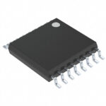 NLVHC4094BDTR2G

NLVHC4094BDTR2G is listed in the Shift Registers range at ChipApex. The manufacturer field lists onsemi. Its product description is IC SHIFT REGISTER 3ST 16TSSOP.…
Read More
NLVHC4094BDTR2G is listed in the Shift Registers range at ChipApex. The manufacturer field lists onsemi. Its product description is IC SHIFT REGISTER 3ST 16TSSOP.…
Read More
NLVHC4094BDTR2G is listed in the Shift Registers range at ChipApex. The manufacturer field lists onsemi. Its product description is IC SHIFT REGISTER 3ST 16TSSOP.…
Read More
NLVHC4094BDTR2G is listed in the Shift Registers range at ChipApex. The manufacturer field lists onsemi. Its product description is IC SHIFT REGISTER 3ST 16TSSOP.…
Read More
NLVHC4094BDTR2G is listed in the Shift Registers range at ChipApex. The manufacturer field lists onsemi. Its product description is IC SHIFT REGISTER 3ST 16TSSOP.…
Read More
NLVHC4094BDTR2G is listed in the Shift Registers range at ChipApex. The manufacturer field lists onsemi. Its product description is IC SHIFT REGISTER 3ST 16TSSOP.…
Read More
NLVHC4094BDTR2G is listed in the Shift Registers range at ChipApex. The manufacturer field lists onsemi. Its product description is IC SHIFT REGISTER 3ST 16TSSOP.…
Read More
NLVHC4094BDTR2G is listed in the Shift Registers range at ChipApex. The manufacturer field lists onsemi. Its product description is IC SHIFT REGISTER 3ST 16TSSOP.…
Read More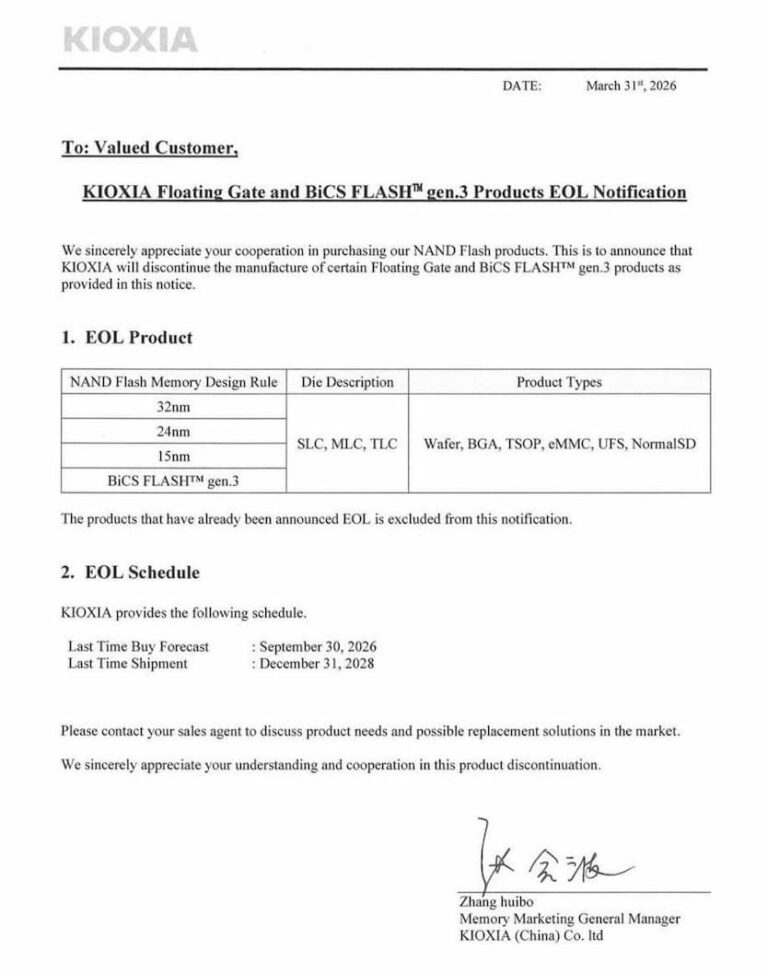
NLVHC4094BDTR2G is listed in the Shift Registers range at ChipApex. The manufacturer field lists onsemi. Its product description is IC SHIFT REGISTER 3ST 16TSSOP.…
Read More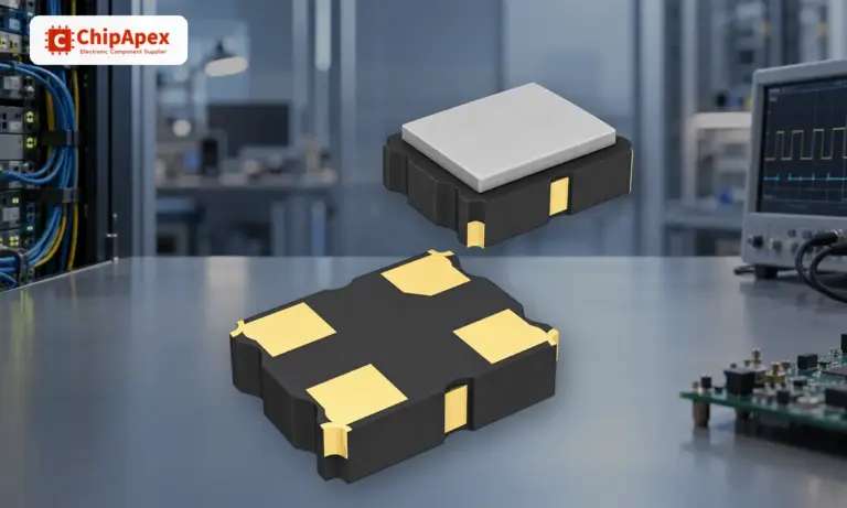
Understand how oscillators generate timing signals, how they differ from crystals, and which frequency, output and stability specs matter when choosing one.
Read More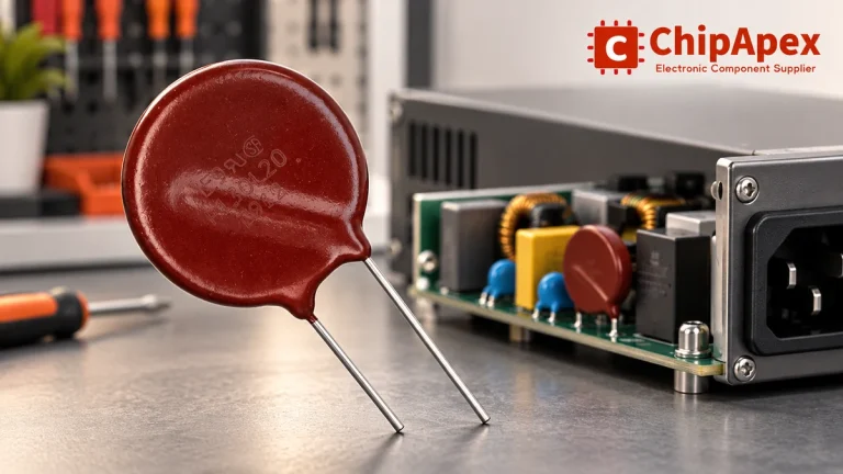
Select MOV varistors by continuous voltage, clamping behavior, surge waveform and repetition. Check thermal disconnection, fuse coordination and replacements.
Read More
NLVHC4094BDTR2G is listed in the Shift Registers range at ChipApex. The manufacturer field lists onsemi. Its product description is IC SHIFT REGISTER 3ST 16TSSOP.…
Read More
The activity of extra discounts on wholesale prices is in full swing…
Please fill in your contact information and we will send you the latest wholesale price list.






