 ChipApex | Global Electronic Components Supplier

SEARCH
Search Product
Search Post
— IC芯片 | 连接器 | 传感器 | 被动器件 —
Search productSearch post
— IC芯片 | 连接器 | 传感器 | 被动器件 —
Consult the customer manager about the wholesale price.
consultation hotline:86-132-6715-2157
email:[email protected]
Contact the product manager for consultation. One-stop consultation is available.
Do you want a lower wholesale price? Please send us your inquiry and we will reply immediately.
NTJD4152PT1G is listed in the FET, MOSFET Arrays range at ChipApex. The manufacturer field lists onsemi. Its product description is MOSFET 2P-CH 20V 0.88A SC88. Review the specifications below when checking this part for your BOM.
The NTJD4152PT1G is a dual P-channel enhancement-mode MOSFET manufactured by onsemi. It features an isolated transistor configuration within a surface-mount US package containing six pins. The device supports a maximum drain-source voltage of 20 V and a continuous drain current of 880 mA. Key electrical parameters include a maximum drain-source resistance of 1 Ω, a typical gate charge of 2.2 nC at the specified gate-source voltage, and a forward voltage of -0.8 V. The component operates within a temperature range from -55°C to 150°C with a maximum power dissipation of 350 mW.
Verify the specific ordering suffix against official manufacturer documentation to confirm exact packaging and tape-and-reel specifications. Ensure that the requested variant matches the required automotive qualification standards if applicable to the design. Cross-reference the component marking with the datasheet to prevent counterfeit substitution during sourcing.
Select this component when a dual P-channel solution is required within a minimal footprint. The 20 V rating suits low-voltage applications, while the 880 mA current capacity supports moderate load requirements. Consider the SOT-363 equivalent package dimensions for PCB layout constraints and thermal management needs relative to the 350 mW dissipation limit.
This part belongs to onsemi's portfolio of small-signal MOSFETs designed for portable electronics. It serves as a complementary device to N-channel counterparts in the same series, offering matched performance characteristics for differential or high-side switching applications. The family emphasizes space efficiency and reliability for mobile and handheld form factors.
Consult official cross-reference lists for verified substitutes. Generic equivalents may differ in gate charge or on-resistance values. Verify pin compatibility and thermal performance before implementation.
The absolute maximum gate-source voltage is ±12 V.
Yes, the device meets the AEC-Q101 automotive standard requirements.
The component is housed in a 6-pin US surface-mount package, commonly identified as SOT-363.
Explore related parts through FETs, MOSFETs, Transistors, Discrete Semiconductor Products, all product categories.
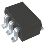 NTJD4152PT1G

The activity of extra discounts on wholesale prices is in full swing…
Please fill in your contact information and we will send you the latest wholesale price list.





