 ChipApex | Global Electronic Components Supplier

SEARCH
Search Product
Search Post
— IC芯片 | 连接器 | 传感器 | 被动器件 —
Search productSearch post
— IC芯片 | 连接器 | 传感器 | 被动器件 —
Consult the customer manager about the wholesale price.
consultation hotline:86-132-6715-2157
email:[email protected]
Contact the product manager for consultation. One-stop consultation is available.
Do you want a lower wholesale price? Please send us your inquiry and we will reply immediately.
The NTLJD3181PZTBG is a dual P-channel MOSFET array manufactured by onsemi, housed in a compact 6-WDFN (2x2) surface-mount package with an exposed pad. Designed for logic-level gate drive applications, this component features a drain-source voltage rating of 20V and a continuous current capacity of 2.2A. Key electrical specifications include a maximum gate threshold voltage of 1V at 250µA, a typical gate charge of 7.8nC at 4.5V, and an input capacitance of 450pF at 10V. The device supports a wide operating junction temperature range from -55°C to 150°C and has a maximum power dissipation of 710mW.
Verify the specific ordering suffix against official manufacturer documentation to confirm exact packaging and reel specifications. Confirm that the component status aligns with project requirements, as availability may vary. Ensure that the 6-WDFN footprint matches the intended PCB layout and thermal design constraints before finalizing procurement decisions.
Select this component when a dual P-channel solution is required for low-voltage applications up to 20V. The logic-level gate threshold simplifies driver circuit design compared to standard threshold devices. Evaluate the thermal performance of the 6-WDFN package against the expected power dissipation levels to ensure reliable operation within the specified temperature range.
This part belongs to onsemi's discrete semiconductor portfolio, specifically within the MOSFET array category. It represents a solution for integrating multiple switching elements into space-constrained designs. The product line focuses on providing efficient power switching capabilities for modern consumer and industrial electronics.
Consult official cross-reference data or manufacturer substitution guides to identify compatible alternatives. Verify that any substitute maintains identical pinout compatibility, voltage ratings, and thermal characteristics to ensure seamless integration without redesigning the host circuit board.
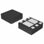 NTLJD3181PZTBG

The activity of extra discounts on wholesale prices is in full swing…
Please fill in your contact information and we will send you the latest wholesale price list.





