ChipApex | Global Electronic Components Supplier

SEARCH
Search Product
Search Post
— IC芯片 | 连接器 | 传感器 | 被动器件 —
Search productSearch post
— IC芯片 | 连接器 | 传感器 | 被动器件 —
Consult the customer manager about the wholesale price.
consultation hotline:86-132-6715-2157
email:[email protected]
Contact the product manager for consultation. One-stop consultation is available.
Do you want a lower wholesale price? Please send us your inquiry and we will reply immediately.
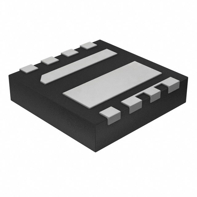
NTLLD4901NFTWG is listed in the FET, MOSFET Arrays range at ChipApex. The manufacturer field lists onsemi. Its product description is MOSFET 2N-CH 30V 5.5A/6.3A 8WDFN. Review the specifications below when checking this part for your BOM.
The NTLLD4901NFTWG is a dual N-channel power MOSFET with an integrated Schottky diode, housed in a WDFN8 (3 mm x 3 mm) package. It features a co-packaged power stage design to minimize board space and parasitic inductances. The top FET (Q1) supports a continuous drain current of 8.3 A at 25°C with a maximum on-resistance of 17.4 mΩ at VGS = 10 V. The bottom FET (Q2) handles up to 9.6 A continuously with a maximum RDS(on) of 13.3 mΩ at VGS = 10 V. Both devices operate with a 30 V drain-to-source voltage rating and are optimized for high-side and low-side switching applications.
Verify the specific ordering suffix 'T' indicates tape and reel packaging containing 3000 units per reel. Confirm RoHS compliance and Pb-free status as documented in the datasheet. Ensure the component matches the WDFN8 CASE 511BP mechanical outline dimensions before integration into the PCB layout.
Select this component for applications requiring a compact dual N-channel configuration with integrated body diodes. Evaluate thermal resistance values based on the specific FR4 pad size used, as steady-state dissipation varies significantly between minimum recommended pads and larger copper areas. Consider gate charge requirements for driving circuitry compatibility.
This part belongs to onsemi's portfolio of co-packaged power solutions utilizing WDFN technology. It integrates two distinct N-channel MOSFETs within a single 3x3 mm footprint, offering a space-efficient alternative to discrete components for synchronous rectification or half-bridge configurations.
Direct substitutes must match the WDFN8 3x3mm package, 30V rating, and dual N-channel topology. Verify pinout compatibility, particularly the shared source/drain connections, and ensure equivalent RDS(on) and thermal characteristics to maintain system performance without redesigning the PCB footprint.
Q1 is designated as the Top FET with a continuous current rating of 8.3 A and higher on-resistance, while Q2 is the Bottom FET rated for 9.6 A with lower on-resistance. Q2 also includes the integrated Schottky diode.
Thermal resistance varies based on the PCB copper area. Using a 1 sq-in pad with 2 oz Cu yields a junction-to-ambient resistance of approximately 68.8 °C/W for Q1, whereas using the minimum recommended pad size increases this to 156.4 °C/W.
No, the datasheet specifies that only the Low Side MOSFET (Q2) has an integrated Schottky diode. Q1 relies on its intrinsic body diode.
Explore related parts through FETs, MOSFETs, Transistors, Discrete Semiconductor Products, all product categories.
 NTLLD4901NFTWG

The activity of extra discounts on wholesale prices is in full swing…
Please fill in your contact information and we will send you the latest wholesale price list.