 ChipApex | Global Electronic Components Supplier

SEARCH
Search Product
Search Post
— IC芯片 | 连接器 | 传感器 | 被动器件 —
Search productSearch post
— IC芯片 | 连接器 | 传感器 | 被动器件 —
Consult the customer manager about the wholesale price.
consultation hotline:86-132-6715-2157
email:[email protected]
Contact the product manager for consultation. One-stop consultation is available.
Do you want a lower wholesale price? Please send us your inquiry and we will reply immediately.
NTMC1300R2 is listed in the FET, MOSFET Arrays range at ChipApex. The manufacturer field lists onsemi. Its product description is MOSFET N/P-CH 30V 2.2A 8SOIC. Review the specifications below when checking this part for your BOM.
The NTMC1300R2 is a complementary dual N- and P-channel Power MOSFET in an SO-8 package. It features a 30 V drain-source voltage rating with continuous drain currents of 2.2 A (N-Channel) and 1.8 A (P-Channel). The device offers ultra-low on-resistance, typically 73 mΩ for the N-Channel and 100 mΩ for the P-Channel at VGS = 10 V. Total power dissipation is rated at 2.0 W at 25°C ambient temperature. The component operates within a junction temperature range of -65°C to +150°C and includes specified avalanche energy capabilities.
Verify the specific ordering suffix and packaging type when sourcing. Confirm that the received components match the manufacturer's marking diagram and pin assignment specifications. Ensure compatibility with standard SO-8 footprint dimensions during PCB layout design to guarantee proper solder connection interface.
Select this component for designs requiring a matched N- and P-channel pair in a compact form factor. Evaluate the thermal resistance requirements based on the intended copper pad area and cooling method. Consider the gate threshold voltage characteristics to ensure compatibility with the driving logic levels used in the target application circuit.
This part belongs to onsemi's Power MOSFET portfolio, specifically categorized as a complementary dual device. It utilizes silicon technology and is housed in the SO-8 surface mount package. The product line targets low voltage switching applications where space constraints and efficiency are critical design parameters.
Check for direct cross-reference part numbers from other manufacturers offering identical complementary N/P channel configurations in SO-8 packages. Verify that substitute devices meet or exceed the 30 V breakdown voltage and current handling capabilities required by the original design specifications.
The maximum continuous drain current for the N-Channel is 2.2 A under steady-state conditions with minimum recommended pad size.
Thermal resistance varies significantly based on the copper area; it ranges from 178.5 °C/W with minimum pads to 62.5 °C/W with larger 1-inch square pads.
Yes, the device features fast switching characteristics with turn-on delay times as low as 9 ns and rise times around 11 ns for the P-Channel.
Explore related parts through FETs, MOSFETs, Transistors, Discrete Semiconductor Products, all product categories.
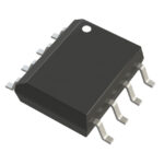 NTMC1300R2

The activity of extra discounts on wholesale prices is in full swing…
Please fill in your contact information and we will send you the latest wholesale price list.





