 ChipApex | Global Electronic Components Supplier

SEARCH
Search Product
Search Post
— IC芯片 | 连接器 | 传感器 | 被动器件 —
Search productSearch post
— IC芯片 | 连接器 | 传感器 | 被动器件 —
Consult the customer manager about the wholesale price.
consultation hotline:86-132-6715-2157
email:[email protected]
Contact the product manager for consultation. One-stop consultation is available.
Do you want a lower wholesale price? Please send us your inquiry and we will reply immediately.
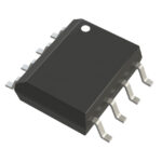
NTMD2P01R2 is listed in the FET, MOSFET Arrays range at ChipApex. The manufacturer field lists onsemi. Its product description is MOSFET 2P-CH 16V 2.3A 8SOIC. Review the specifications below when checking this part for your BOM.
The NTMD2P01R2G is a dual P-channel MOSFET manufactured by onsemi, housed in an SOIC-8 surface-mount package. It features a drain-source breakdown voltage (Vds) of 20 V and a continuous drain current (Id) of 5.07 A. The device exhibits a low on-resistance (Rds(on)) of 35 mΩ at Vgs = -4.5 V. Gate-source voltage limits are ±12 V, with a threshold voltage (Vgs(th)) of 1.2 V. Total gate charge (Qg) is 12 nC. Power dissipation is rated at 2 W, operating within a temperature range of -55°C to +150°C.
Verify the component suffix 'G' indicates RoHS compliance when sourcing. Confirm the manufacturer designation as onsemi to ensure authenticity. Check datasheet revisions for any updates to thermal resistance or electrical limits before finalizing procurement specifications.
Select this part for applications requiring a 20 V rating with high current capability in an 8-pin footprint. Ensure the driving circuit can supply sufficient negative gate voltage to fully enhance the P-channel devices. Verify that the PCB layout supports the required thermal dissipation for the specified power rating.
This component belongs to the NTMD6N02/NTMD6P02 series of dual MOSFETs from onsemi. It serves as the P-channel counterpart to N-channel variants, providing matched characteristics for half-bridge or full-bridge topologies. The series is designed for general-purpose power switching in consumer and industrial electronics.
The NTMD6P02R2G is a compatible alternative offering identical pinout and electrical specifications. Verify package dimensions and thermal performance match the existing design constraints before substitution.
The absolute maximum rating for gate-source voltage is ±12 V. Exceeding this limit may damage the gate oxide layer.
While onsemi offers automotive-grade versions of similar MOSFETs, specific qualification for the NTMD2P01R2G must be confirmed via the official datasheet or AEC-Q101 certification status.
Integrating two channels reduces board space and simplifies assembly compared to using discrete single MOSFETs, while ensuring matched thermal and electrical behavior between the pair.
Explore related parts through FETs, MOSFETs, Transistors, Discrete Semiconductor Products, all product categories.
 NTMD2P01R2

The activity of extra discounts on wholesale prices is in full swing…
Please fill in your contact information and we will send you the latest wholesale price list.





